In the process of electrical design, certain design choices must be made. One example is the design of USB Type-C connectors using bridge connectors. In this case, the overall thickness of the PCB is limited by the thickness of the bridge connector. Historically, the standard PCB thickness is 0.063 in (1.57 mm).
Before the advent of PCBs, transistor-based electronic devices were typically assembled using a method known as breadboarding, which involved using wood as a substrate. However, wood is fragile, leading to a very delicate assembly process. To address this issue, the rubber wood board, commonly used as a workbench surface, became the standard substrate for electronic components, with a thickness of 1/16 in, marking the beginning of this thickness of PCBs.
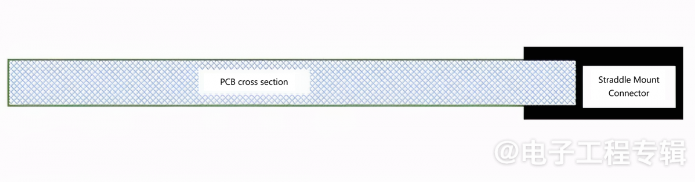
Figure 1: Cross-section of a PCB with a bridge connector. (Source: Wurth Elektronik)
Taking the USB 3.1 plug from Wurth Elektronik as an example, which is a bridge connector with part number 632712000011. The device datasheet recommends a PCB thickness of 0.8 mm / 0.031 in for optimal performance. This thickness of PCB is common among various PCB manufacturing plants. A 0.031 in circuit board is relatively easy to manufacture since many PCB manufacturers produce 6-layer PCBs with 1 oz copper per layer.
However, designing and using thin PCBs also presents several challenges. One major issue is their mechanical fragility. Thin PCBs are softer and more prone to bending or warping, making them difficult to handle during assembly and more susceptible to damage during handling. The handling process includes pick-and-place assembly, drilling, in-circuit testing (ICT), and functional probe testing during functional testing.
The secondary handling is performed by the end user, such as dropping devices that contain PCB assemblies (PCBA). Additionally, thin PCBs often require specialized manufacturing processes and materials, leading to increased production costs. Component placement also becomes more critical, as routing may need to be closer, increasing the risk of short circuits and signal interference.
Furthermore, thin PCBs face challenges in heat dissipation due to reduced thermal mass. To address these challenges, careful consideration must be given during the design, manufacturing, and assembly stages to ensure the reliability and performance of the final product.
When designers install ball grid array (BGA) devices on a 0.031 in thick circuit board, these issues become particularly critical. Most major manufacturers recommend a minimum thickness of 0.062 in when installing BGAs on circuit boards.
How to Test Durability
The mechanical durability of PCB assemblies is generally assessed through drop testing. The requirements for drop testing PCBA typically include specifying the drop height, drop surface, number of drops, drop direction, acceptance criteria, and testing standards. The drop height is the distance from which the PCBA is dropped, usually ranging from 30 to 48 in, depending on the application and industry standards.
Additionally, the drop surface must be determined, such as concrete or wood. Manufacturers specify the number of drops that the PCBA must withstand, typically 3 to 6 times. Furthermore, the direction of the PCBA during the drop process is specified, whether face down, face up, or on an edge or corner. Acceptance criteria, such as functionality after drops and any visible damage, are also clearly defined.
Testing standards such as IPC-TM-650 or specific customer requirements will guide the testing process. For medical devices, drop test requirements are specified in IEC 60601-1 Third Edition 2005-12, Section 15.3.4.1. By establishing these requirements, manufacturers can ensure that their PCBAs and products are sufficiently robust and durable to maintain functionality even after drops and impacts.
During drop testing, solder joints may not be detected until functional failure is observed. BGAs may fail due to assembly-related issues such as thermal stress during soldering or poor solder joint quality. Thin circuit boards can weaken due to excessive mechanical shock and vibration during assembly.
These defects can be identified during drop testing, as BGA components may not withstand the stresses encountered during the drop test. X-ray, optical inspection, or electrical testing can be used to check for BGA failures. Detailed analysis can be performed through cross-sectional analysis using a scanning electron microscope (SEM).
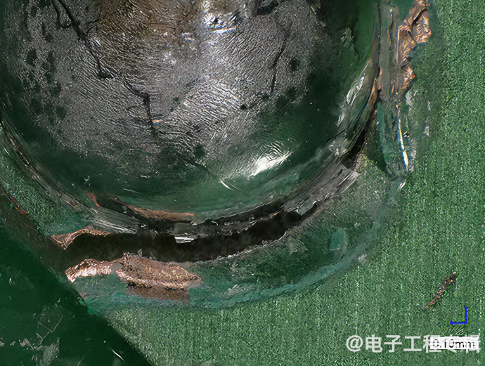
Figure 2: BGA solder joint showing micro-cracks. (Source: Keyence)
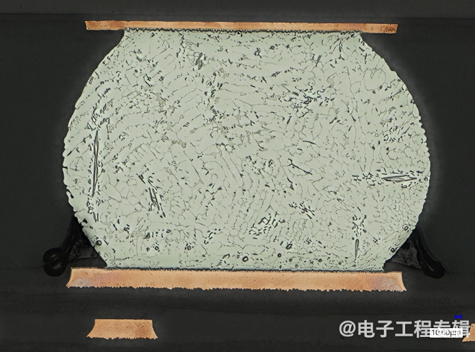
Figure 3: Cross-sectional schematic of a healthy BGA. (Source: Keyence)
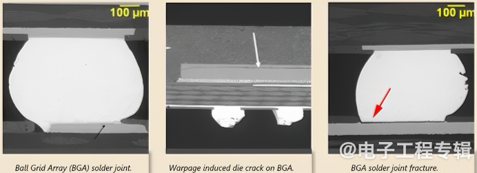
Figure 4: Views of various BGA failure modes. (Source: Semlabs)
How to Repair BGA Failures on Thin PCBs
Pad sinking refers to the cracking of the laminate beneath the copper pad of surface-mount components, which usually occurs during mechanical events. The initial crack can propagate, affecting adjacent copper traces, resulting in an electrical open circuit. This is more common in lead-free components due to different laminate materials. Mitigation measures include reducing stress on the laminate or using stronger, more pad-sink resistant materials.
This issue can be resolved by mechanically stretching the PCB or replacing the laminate material. Any of the following steps can be taken.
-
Thinner circuit boards are more prone to warping and may require additional fixtures (reinforcements or workbench supports) to process on the production line if they do not meet the following requirements. PCB reinforcements are not part of the circuit board itself but are external structures that provide mechanical support to the circuit board.
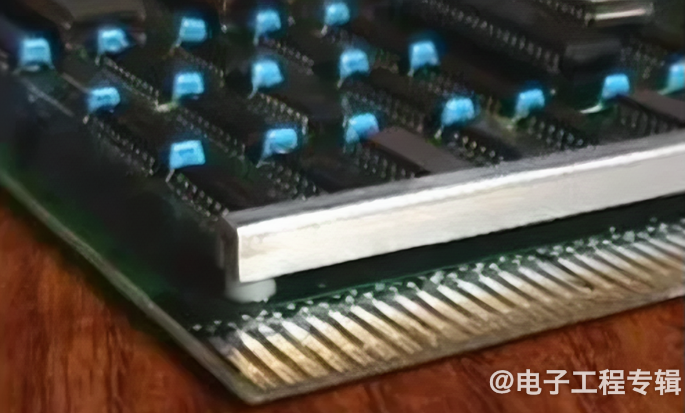
Figure 5: Aluminum bars used as mechanical PCB reinforcements. (Source: Compufab)
-
Use corner adhesives/epoxy at the corners of the BGA or use BGA bottom fillers. For this purpose, adhesives like Zymet UA-3307-B Edgebond, Korapox 558, or Eccobond 286 can be used. Epoxy along the corners of the BGA or as a bottom filler can enhance the strength of the PCB, preventing it from bending and thus preventing failures.
-
Strictly limit PCB bending during circuit board assembly operations. For example, support the PCB during through-hole drilling, pick-and-place, ICT, or functional testing using flying probes.
-
Match the recommended BGA soldering profile. Failing to solder according to the BGA manufacturer’s recommended soldering profile can lead to cold solder joints, exacerbating problems. Sufficient thermocouples should be present on the PCB panel to monitor the PCB temperature.
-
Ensure that the BGA pad size meets the manufacturer’s recommendations.
Addressing the Challenges of Thin PCBs
Thin PCBs (0.031 in) weaken PCB assemblies, making them susceptible to mechanical and thermal forces. Unique challenges arise when installing BGAs on thin PCBs.
However, by carefully controlling the PCB handling processes and then using the design solutions discussed in this article to reinforce thin PCBs, design challenges and risks can be managed.
Editor’s Note: The views expressed in this article are solely those of the author.
Jagbir Singh is an electrical engineer responsible for robotics at Smith & Nephew.
(Originally published on EE Times sister site EDN, reference link: Thin PCBs: Challenges with BGA packages, translated by Franklin Zhao.)