01 Introduction
This article is a translation of the article with the same name published by the “Electronic Chief Intelligence Officer” editorial team of “Printed Circuit Board Information”. The full text is as follows.
To meet the demands of the new generation of high I/O semiconductor packaging, significant changes have occurred in the manufacturing processes and substrate selection standards of printed circuit board technology. The reasons behind these changes are the higher requirements for the number of terminals and terminal spacing posed by the new generation of high-performance semiconductor packaging series.
The interconnection of ultra-fine pitch and high I/O semiconductors significantly impacts PCB design and assembly processes. PCBs with higher interconnection density facilitate the seamless integration of high I/O semiconductor packages in higher-end electronic products. While the complexity of a large number of semiconductor packages (I/O and terminal spacing) is within controllable limits, the I/O density of other packages may be higher. To address conductor routing obstacles, blind via technology is employed, transferring most interconnections below the surface of the circuit board, as shown in Figure 1.
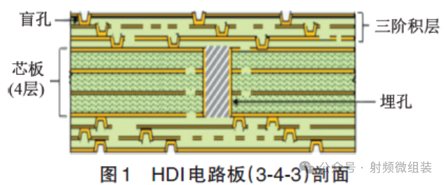
Adjusting blind and buried vias and providing predefined routing channels help PCB designers simplify effective routing for common ultra-fine pitch, array terminal configuration semiconductor packages.
02 Planning for Sequential Build-Up Processing
Sequential build-up (SBU) processing offers various design options. PCB designers can choose to use stacked microvias in sequential build-up or staggered microvias (where vias are offset from one layer to another for inter-layer interconnection). The complexity of SBU PCBs ultimately depends on component density, circuit interconnection density, the number of signal conductor layers, and the number of layers dedicated to power and ground.
The combination order of circuit board layers (signal layers, power layers, ground layers, etc.) is a key factor affecting signal transmission performance. In addition to performance issues, controlling manufacturing costs is also a top priority. For example, the number of layers and the interconnection methods between the selected circuit layers significantly impact the control of process complexity. To achieve inter-layer interconnection, blind via technology is employed, which will significantly increase circuit routing density. Additionally, the build-up process also has a significant impact on manufacturing complexity, affecting the number of laminations. Any starting layer of microvias must be precisely aligned with the connection pad pattern to ensure effective connections between layers through the interface. However, during each lamination cycle, the core material undergoes repeated high-temperature and high-pressure tests, which may lead to material decomposition.
03 Controlling HDI and UHDI Manufacturing Costs
The complexity level of a PCB is determined by the number of signal layers and power/ground layers required for interconnection. By adopting finer routing and spacing, small microvias, and innovative multilayer approaches, PCB designers can overcome many interconnection challenges posed by the new generation of semiconductors. When defining the complexity level of high-density interconnect (HDI) or ultra-high-density interconnect (UHDI) PCBs, designers first establish standards for manufacturing the circuit board, including shape and thickness limitations. To ensure that the circuit board thickness meets the restrictions, clear targets must be established to determine the number of circuit layers dedicated to signal routing and the number of layers reserved for power and ground distribution. While power and ground may only require two circuit layers, the number of required signal layers is determined by component density and interconnection complexity.
When assessing PCB design complexity, the first consideration is the ratio of component area to circuit board area. If the surface area of the component interface is limited, multilayer HDI manufacturing can be employed. To ensure the successful production of HDI, designers must recognize the complexity of the manufacturing process and the associated cost impacts when implementing more complex manufacturing procedures. Early planning of conductor routing schemes, separating the connection pads of through vias, microvias, and/or component connection pads, is essential. The width of the routing channels will be calculated using the terminal pitch (the center-to-center distance) and the size of the connection pad pattern, thereby determining the maximum number of conductors that can be routed between each channel (the number of conductors per channel). When the above channels are further restricted, designers need to consider routing circuits below the surface of the circuit board to achieve interconnection.
The industry’s development roadmap continues to emphasize that improving materials and processes is key to enhancing product performance and manufacturing efficiency. The laminate industry is making significant improvements to all packaging and substrate-related materials. For HDI applications, the selected substrate must have sufficient mechanical stability to withstand the process temperatures experienced during PCB manufacturing and throughout the assembly process. While multilayer circuit board manufacturing is a mature and widely available service, the process sequences and methods may vary among suppliers. The complexity of components and circuits requires higher density circuit layouts, and PCB manufacturers possess the expertise to provide circuit boards capable of achieving higher density circuits. However, physical limitations often restrict the interconnection potential of circuit boards: 1) Limited PCB surface area; 2) High component density ratio; 3) Larger semiconductor I/O; 4) Ultra-fine pitch terminal spacing.
As semiconductor product manufacturing becomes increasingly complex, employing HDI technology helps address many challenges that arise during production. In circuit board design, factors limiting circuit interconnection routing capabilities include: 1) The spacing/distance between microvias or plated through holes; 2) The number of wires routed between connection pad pattern features; 3) The number of designated signal layers.
By effectively utilizing small diameter microvias and more stages of multilayer manufacturing technology, most interconnection challenges can be addressed.
04 Improvements in HDI and UHDI Processes
Improvements in PCB manufacturing processes include achieving more efficient imaging capabilities and greater utilization of alternative hole-making technologies, employing more advanced etching and plating chemical technologies, and improving lamination methods. PCB manufacturing companies with stronger technical capabilities can produce conductors as narrow as 25μm, but they rely on dielectric materials equipped with extremely thin copper foil. When further reducing line width and spacing is required, manufacturers may choose substrates specifically prepared for semi-additive plating processes. Different suppliers exhibit varying levels of process maturity in manufacturing HDI or UHDI circuits. A comparison of the general process objectives for subtractive, semi-additive, and full additive copper deposition, as well as the process differences in microvia formation methods, is shown in Table 1.
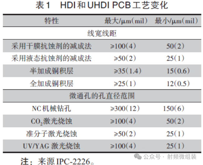
The key factor in achieving higher density circuits is the advancement of imaging technology. Laser direct imaging (LDI) and diode imaging systems have become mainstream technologies in the PCB manufacturing industry. While semi-additive circuit manufacturing has achieved finer circuit geometries, compared to alternative processes offered by specialized suppliers, it can achieve full additive copper deposition for finer copper conductor geometries.
05 Supplier Communication
Developing HDI or UHDI is not an easy task. The complexity of materials and processes plays a significant role in the manufacturability and direct costs of multilayer circuit boards. Among the challenges is selecting the most suitable substrate for applications while meeting the electrical and operational environment requirements of the end product. For PCB designers, it is recommended to communicate with PCB manufacturing professionals at the early stages of each new design. Although numerous guidelines for high-density and sequential laminated circuit board design are provided in publications and standards documents from the Institute of Printed Circuits (IPC), PCB suppliers ultimately become the most meaningful assurance for designers to ensure end product satisfaction.
Regarding manufacturing process efficiency and meeting PCB cost targets, manufacturers encourage designers to evaluate the overall structure of the circuit to simplify the design. As mentioned earlier, reducing line width and spacing can effectively reduce the number of layers. In terms of implementing SBU technology, the most expensive stacking configurations require multiple consecutive laminations. Therefore, reducing the stacking of circuit layers on both sides of the circuit board has a very positive impact on controlling unit costs.
06 New Guideline Standards for HDI and UHDI
IPC-2226 defines HDI as having a wiring density per unit area higher than traditional PCBs, with finer line widths and spacings (≤100/100μm), smaller vias (<150μm) and capture pads (<400μm), and higher connection pad densities (>20/cm2) compared to traditional PCB technology. UHDI is defined as having conductor widths, insulation distances, and dielectric thicknesses all less than 50μm, with microvia diameters less than 75μm, exceeding the existing IPC-2226 standards.
Jan Pedersen from the NCAB Group noted that his company “receives daily inquiries about PCBs with conductor widths and insulation distances less than the current requirements for standard HDI boards.” Pedersen, who initially served as the chairman of the IPC Medical Committee, discussed the updated requirements and parameters needed for future generations of semiconductor components that require higher density circuit boards. However, when customers do not provide basic rules during the design phase, factories cannot manufacture PCBs. To improve factory capacity, it is essential to ensure production meets standards.
With the gradual development of UHDI technology, a technical working group approved by the IPC Technical Activities Executive Committee and composed of member companies has begun work. This group has spent three years planning and has developed two new standards for UHDI circuits, namely IPC-2229 and IPC-6019, which will serve as guidelines for PCB design engineers and manufacturers in the current and future manufacturing of HDI circuit boards. The committee aims to release these standards by the end of 2025.
★★★Recommended Classic Books in the Industry★★★
Advanced packaging is the direction of RF technology development and is of great significance for the miniaturization and high reliability of RF modules. This public account shares a wealth of technical research and products related to advanced packaging. We hope everyone learns from the advanced ideas in the industry and draws on the advanced experiences in the industry. Here are a few excellent books from both domestic and international sources that we hope everyone can look at the world and learn and progress while standing on the shoulders of giants.
In the current competitive industry, engineers face heavy work pressure and must also balance family responsibilities in their spare time, making it difficult to devote a lot of energy to literature research. Therefore, this public account has carefully organized research literature in related fields to build a convenient academic exchange platform. We always adhere to the principle of respecting intellectual property rights and express our deep respect for the academic contributions of each original author. If any content has copyright issues, please contact the public account in a timely manner for deletion.
|
【Previous Articles Recommended for Reading】 Research Progress on RF Integrated Applications of Glass Through Hole Technology Research on BGA Solder Ball Isolation Performance in 3D SiP Modules Design of a Miniaturized Ultra-Wideband Dual-Band Receiving RF Front-End Process Control of Sulfide Failure in Chip Resistors for Aviation Use Optimization of Chemical Nickel Plating Process for Aluminum Oxide Ceramic Packaging Design and Implementation of High-Performance Miniaturized Intermediate Frequency LC Filter Research on Control of Solder Splash Residue in Surface Acoustic Wave Filters A Process Method for Secondary Parallel Sealing Research on Welding Process Technology for Ceramic Dielectric Filters Research on High Reliability LC Filter Assembly Process Based on Integrated Packaging of Ceramic Substrates Design of a Broadband Miniaturized Phase-Locked Source Based on SiP Technology A Design of a Low-Loss Millimeter-Wave Front-End Module for BGA Packaging Design and Implementation of a Miniaturized Four-Channel Antenna Interface Unit for K Band Research on Efficient Cleaning Process Methods for Microwave Transceiver Components Based on Ceramic Packaging A Transmitter Component with Precise Control of Output Power Analysis of RF Transmission Characteristics Based on CCGA Research and Application of Laser Marking Solder Mask Technology on T/R Components Design and Implementation of S-Band GaN High-Power Front-End Components Research on the Reliability of BGA Interconnections Based on Silicon-Based Heterogeneous Integration |
To learn more about cutting-edge RF information, please follow the public account