Documenting work, sharing experiences, and open-sourcing! Speed up!  Committed to ensuring that every step of our design is theoretically supported! Bookmark and follow to progress together.


 Please pay attention to the comments section, as some colleagues will discuss and supplement there, enriching this theoretical library together!
Today, I will share an essential skill for high-speed design: Ground Via Design!
Ground vias provide a return path for signals at vias. Increasing the number of ground vias can further improve performance;
Here’s a comparison image to help with understanding.
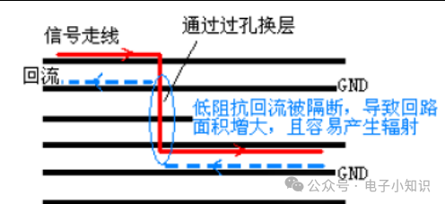
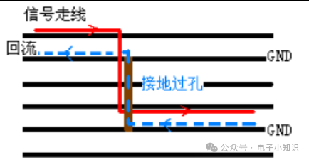
Ground via requirements: For signal rates >5Gbps, ground vias must be used; for signal rates ≤5Gbps, there are no requirements, but it is recommended to use ground vias if space allows.
The center-to-center distance between ground vias and signal vias: P=35mil~40mil, depending on the board density.

As usual: Old friends like, new friends follow, and continue to share PCB practical skills to enhance the value of technical personnel!
Forming a theoretical knowledge discussion group! Note: Discussion group!