Chip Design | Basic Concepts (Part 8) Terminology Related to Tape-Out

Chip Design | Basic Concepts (Part 8) Terminology Related to Tape-Out

Tape-out refers to the delivery of the final design data to the foundry for initial production, which is the most milestone-significant and also the most “costly” phase in the chip design process. 1. Decisions and Verification Before Tape-Out 1. MPW Full Name: Multi-Project Wafer Chinese: 多项目晶圆 Explanation: A method to reduce tape-out costs. It involves … Read more

Latest Breakthroughs in China’s Chip Industry

Photolithography technology is one of the core driving forces behind the continuous miniaturization of integrated circuit chip manufacturing processes. According to the Science and Technology Daily, recently, Professor Peng Hailin’s team from Peking University’s School of Chemistry and Molecular Engineering, along with collaborators, successfully utilized cryo-electron tomography to analyze the microscopic three-dimensional structure, interfacial distribution, … Read more

Only 5 Metal Atoms per Square Centimeter! The “Cleanliness” Standards of Semiconductor Cleaning Hide the Secrets to Chip Yield

In semiconductor factories, the cleaning process has a set of “extremely strict” standards: since 2013, the number of metal atoms on the surface of each square centimeter of a wafer cannot exceed 0.5×10¹⁰ (equivalent to allowing only 5 soccer balls on a soccer field), the diameter of particles on the back must be less than … Read more

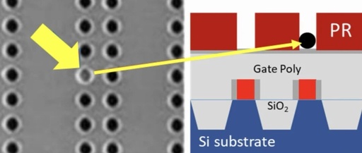
Defect Cases in Semiconductor Evaporation Processes / Common Defect Types in Practice

Defect Cases in Semiconductor Evaporation Processes / Common Defect Types in Practice

Table of Contents [CH.1]: Shallow Trench Isolation (STI) Gapfill Defects [CH.2]: Seam Defects [CH.3]: Particle-Induced Defects [CH.4]: Deposition Uniformity Defects [CH.5]: Silicide Encroachment / Silicide Stringer Defects [CH.6]: Overhang Defects [CH.7]: Poor Step Coverage Defects [CH.8]: Cracking Defects in Insulating Films [CH.9]: Gate Oxide Thinning Defects [CH.10]: Not Open Defects [CH.1] Shallow Trench Isolation (STI) … Read more

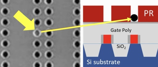
Defect Cases in Semiconductor Evaporation Processes / Common Defect Types in Practice

Defect Cases in Semiconductor Evaporation Processes / Common Defect Types in Practice

Table of Contents [CH.1]: Shallow Trench Isolation (STI) Gapfill Defects [CH.2]: Seam Defects [CH.3]: Defects Caused by Particles [CH.4]: Deposition Uniformity Defects [CH.5]: Silicide Encroachment / Silicide Stringer Defects [CH.6]: Overhang Defects [CH.7]: Poor Step Coverage Defects [CH.8]: Cracking Defects in Insulating Films [CH.9]: Gate Oxide Thinning Defects [CH.10]: Not Open Defects [CH.1] Shallow Trench … Read more

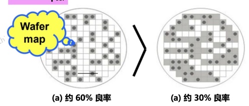
Understanding Semiconductor Yield: Techniques for Yield Improvement

Understanding Semiconductor Yield: Techniques for Yield Improvement

Table of Contents CH.1 “Yield” in the Semiconductor Industry CH.2 Categories of Semiconductor “Yield” CH.3 Components of Yield CH.4 Reasons for Low EDS Yield CH.5 Characteristics of Different Yields CH.6 Methods for Analyzing Poor Yield CH.7 EMMI Analysis in Electrical Failure Analysis CH.8 Why Yield is Important★Important★ CH.9 Solutions for Improving Productivity CH10. The Relationship … Read more

Samsung’s US Chip Factory Faces Challenges: $37 Billion Investment at Risk Due to Customer Shortage

Samsung's US Chip Factory Faces Challenges: $37 Billion Investment at Risk Due to Customer Shortage

On July 4, according to Nikkei Asia, sources revealed that South Korean chip manufacturer Samsung Electronics is delaying the completion of its semiconductor factory in Texas, USA, due to difficulties in finding customers for the factory’s products. Previously, Samsung announced plans to invest over $37 billion (approximately 265.03 billion RMB at current exchange rates) in … Read more

Decoding Semiconductor Jargon: From CD to GAA, the ‘Secret Codebook’ of Chip Manufacturing

Decoding Semiconductor Jargon: From CD to GAA, the 'Secret Codebook' of Chip Manufacturing

Senhui Introduction: Suzhou Senhui Semiconductor, supported by a strong research and technology team, focuses on providing complete process solutions and wafer fabrication services for global compound semiconductor customers. The company team members have deep experience in the semiconductor industry, with decades of rich capabilities in photolithography, thin film processes, epitaxy, bonding processes, as well as … Read more

Chip Industry Faces Challenges: Tape-out Success Rate Drops to 14%

Chip Industry Faces Challenges: Tape-out Success Rate Drops to 14%

According to reports from Fast Technology, the semiconductor industry is facing unprecedented technical challenges, with the tape-out success rate for chips dropping to a historic low! Data from Siemens, an Electronic Design Automation (EDA) company, shows that the success rate of the first tape-out (tape-out) for chips has fallen to a historic low of 14%, … Read more