Table of Contents
[CH.1]: Shallow Trench Isolation (STI) Gapfill Defects
[CH.2]: Seam Defects
[CH.3]: Particle-Induced Defects
[CH.4]: Deposition Uniformity Defects
[CH.5]: Silicide Encroachment / Silicide Stringer Defects
[CH.6]: Overhang Defects
[CH.7]: Poor Step Coverage Defects
[CH.8]: Cracking Defects in Insulating Films
[CH.9]: Gate Oxide Thinning Defects
[CH.10]: Not Open Defects
[CH.1] Shallow Trench Isolation (STI) Gapfill Defects
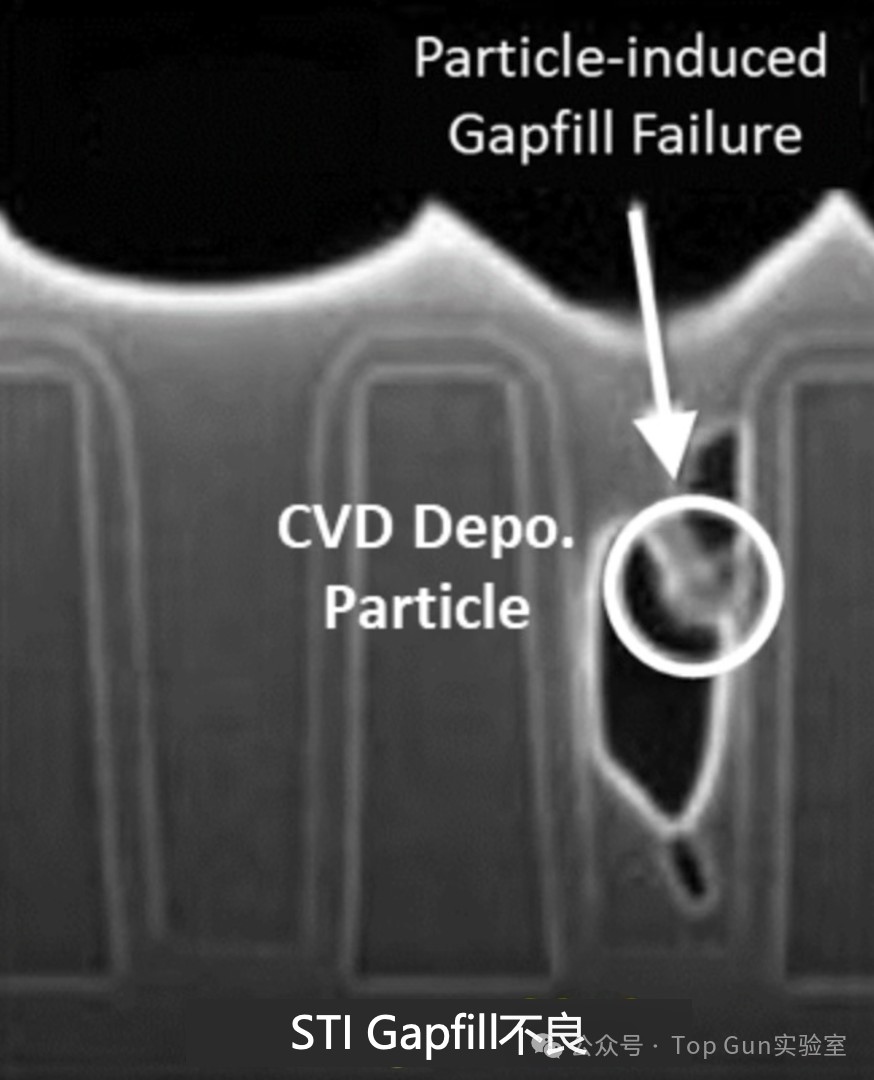
The first type of defect issue is the poor filling of STI (Shallow Trench Isolation). The isolation process can be divided into trench isolation and junction isolation. Particularly for trench isolation, it defines the transistor device domain by physically separating adjacent devices while also providing electrical isolation. However, during the formation of STI, if the deposition process capability is insufficient as shown in the figure, due to overhang at the opening or particles within the trench profile, incomplete gapfill will occur, leading to the formation of voids, which causes field leakage between adjacent devices. This results in increased device characteristic dispersion or mismatch; in severe cases, the device may experience hard failure and cease to function properly. As the process continues to shrink, the demand for high-difficulty gapfill technology in deposition processes is increasing.
[CH.2] Seam Defects
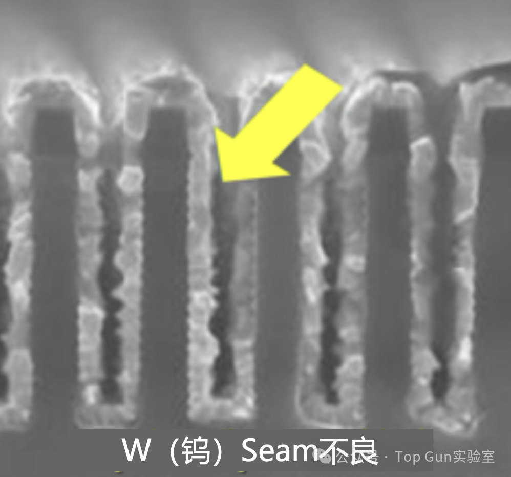
The second defect is seam defects. Seam and void share a common characteristic of being defects caused by a decrease in gapfill capability due to high aspect ratio (High AR) and poor step coverage. (They can be simply understood as morphological differences; when seam gaps become severe, they evolve into voids). Especially in advanced processes, to achieve high density and multifunctionality within a single chip, countless transistors (Tr.) are integrated into the IC. To realize their electrical functions, a large number of contacts/vias and complex metal routing must be formed. Therefore, the contact/via holes formed to connect the metal lines between upper and lower layers increasingly exhibit high aspect ratio profiles. If, as shown in the figure, tungsten (W) metal is not properly filled (gapfill), it will lead to increased resistance, resulting in failure. Thus, a high-difficulty deposition process technology with excellent step coverage characteristics is required.
[CH.3] Particle-Induced Defects
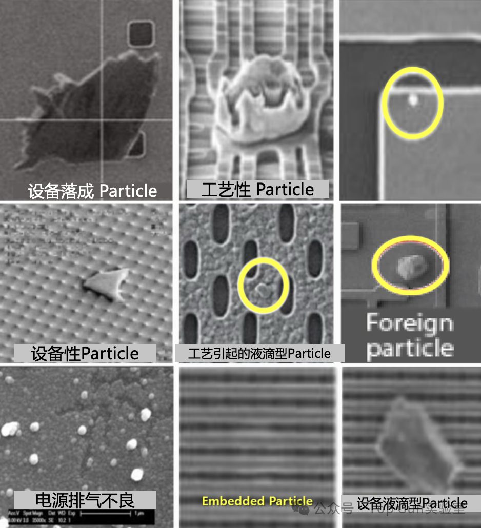
Defects caused by particles typically present a random distribution on the wafer map, most manifesting as hard failures (Hard Fail), thus requiring enhanced Continuous Improvement Processes (CIP) to reduce particle occurrences. Particle defects generally lead to short circuits between metal lines or voids in contact/via holes, resulting in open failures. Additionally, if deposition processes occur in the presence of particles, under bias or during deposition, the areas with particles may release stress or volatile gases, leading to pinhole defects. Since defects caused by particles are mostly hard failures (Hard Fail), aside from maintaining a clean manufacturing environment, there are few other remedial measures. Moreover, they account for a significant portion of yield loss, making them critical.
Typically, particle defects can be classified into three categories: 1. Equipment-induced particles, 2. Process-induced particles, 3. External particles. As inferred from the figure, equipment-induced particles generally appear at the wafer edge, indicating improper preventive maintenance (PM) and exhaust conditions of the equipment, necessitating a re-examination of equipment input parameters. Particles generated during the process reaction usually exhibit a round shape, possibly due to equipment failure or unoptimized process conditions. The last type is non-reactive or equipment-induced but originates from external environmental particles. When photolithography patterns are formed over particles, the particles remaining beneath the patterned film can cause step height differences, affecting the integrity of the upper pattern. Therefore, the PM cycle of the equipment, optimization of process conditions, and a clean process environment are all key to controlling particle defects.
[CH.4] Deposition Uniformity Defects
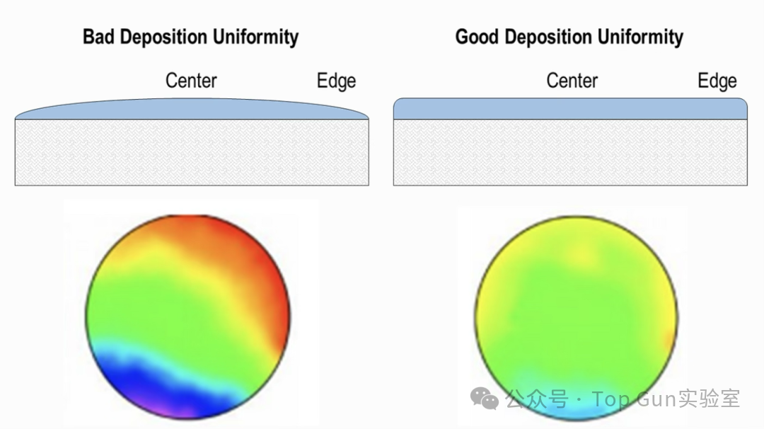
Poor uniformity on the wafer during the deposition process can lead to variations in device characteristics and cause defects such as open/short failures in subsequent processes. Process engineers need to optimize deposition conditions such as temperature and pressure in the process recipe while improving uniformity at various positions on the wafer, such as L/B/C/T/R/LT/LB/RB/RT. In other words, optimizing uniform deposition rates based on wafer position is the responsibility of deposition process engineers. The uniformity between the wafer center and edge is crucial not only in the deposition process but also poses key challenges in photolithography, chemical mechanical polishing (CMP), and etching processes. Especially with the advent of fine processes, its importance is further heightened.
[CH.5] Silicide Encroachment / Silicide Stringer Defects
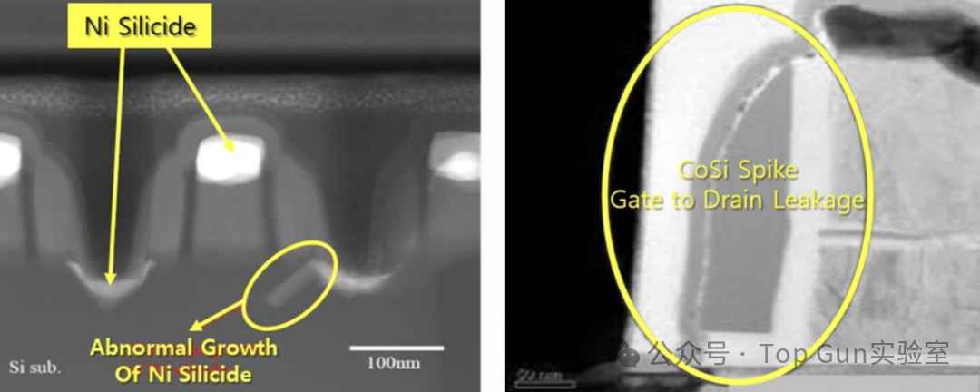
The silicide process is aimed at reducing the high contact resistance caused by the Schottky barrier formed due to the work function difference between metals and semiconductor junctions. The basic process of the so-called self-aligned silicide (Salicide) can be briefly described as follows: First, Co/Ti/Ni metals and a capping layer are deposited overall on the wafer surface through physical vapor deposition (PVD), followed by annealing to allow metal atoms to diffuse into the silicon and form a silicide layer. However, in actual processes, silicide may exhibit abnormal growth (encroachment), leading to junction leakage in devices. This issue is often significantly influenced by silicon substrate doping, surface cleaning, Ni film thickness, and annealing conditions. The silicide stringers shown in the right figure refer to silicide residues remaining on the device sidewalls. Such residues can also form leakage paths between the gate and drain, thereby affecting device performance.
[CH.6] Overhang Defects
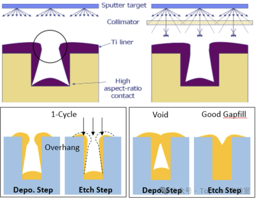
When overhang occurs, it can lead to the formation of voids below in severe cases. In PVD processes, to improve overhang issues, collimators are typically used. However, during collimated sputtering, particles can deposit on the collimator, leading to a decrease in deposition rate, necessitating regular replacement. In CVD processes, HDPCVD (High-Density Plasma Chemical Vapor Deposition) is often used to address overhang issues, implemented through a Depo-Sputtering 1-Cycle method, commonly applied in trench processes. However, due to excessively high plasma density, defects caused by plasma damage may arise, potentially leading to hump phenomena and variations in device characteristics and mismatch. Therefore, to densify the STI (Shallow Trench Isolation) films, it is necessary to perform densification treatments in subsequent processes.
[CH.7] Poor Step Coverage Defects
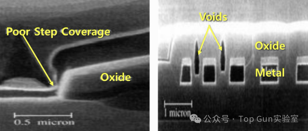
To enhance step coverage, it is necessary to reassess the deposition recipe for interlayer dielectric (ILD) films and replace materials to achieve void-free processes.
[CH.8] Cracking Defects in Insulating Films
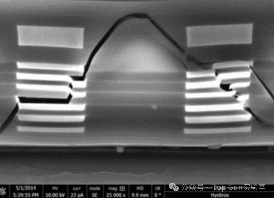
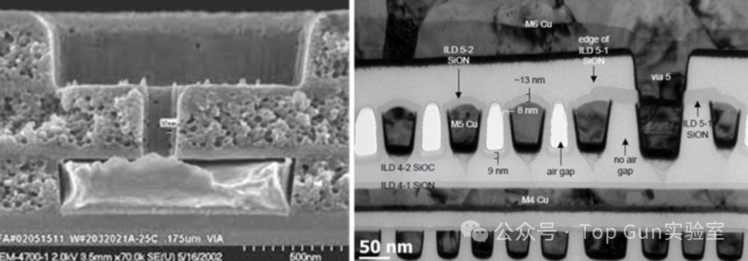
Insulating films play a crucial role in inter-device isolation and other aspects. Especially with the development of fine processes, to reduce the RC delay of metal line signal transmission, low-k materials are adopted in the ILD/IMD layers. These materials achieve low dielectric constants by doping carbon or artificially forming porous structures or even airgaps. However, due to the presence of porous structures, these materials are mechanically very fragile and prone to cracking defects.
[CH.9] Gate Oxide Thinning Defects
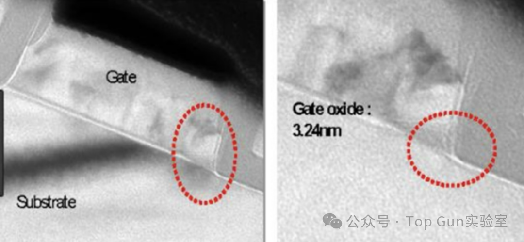
The thickness of the Gate Oxide is one of the critical parameters determining the device’s Gox BV (Breakdown Voltage), reliability, and Vth (Threshold Voltage) characteristics. As mentioned, the localized thinning of the Gate Oxide during specific LOT processes requires strict inspection for abnormalities before and after the process. (Due to its critical impact on device characteristics, this will inevitably affect the normal operation of the product.)
[CH.10] Not Open Defects
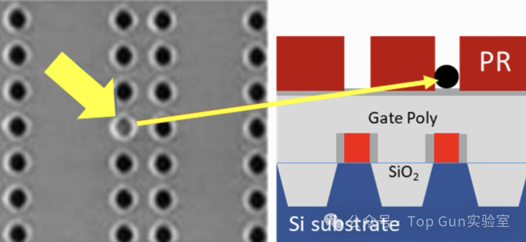
Not Open defects are one of the typical types of hard failures in semiconductor chips. When a specific contact exhibits a Not Open phenomenon, various potential causes must be considered, including particle factors, photo alignment issues, deposition uniformity, and etch uniformity. To prevent such hard failures in layout design, it is advisable to prohibit single contact/via holes and instead form double or more contact/via holes to improve yield loss caused by hard failures. However, increasing a single contact/via to multiple ones may lead to an increase in chip size, thereby reducing design competitiveness.
*Content edited by the team. If you are satisfied, please follow me.
Your attention is my motivation. Thank you*
Recommended Reading
[Second Communication Chip] Innovations in the 5G Era: The Rise of Next-Generation RF Chips POI-SAW and TF-SAW, Challenging the Dominance of Traditional SAW/BAW Filters!
[Semiconductor Photolithography Materials] Uses and Production Processes of Mask Plates Reticle & Photomasks
[Semiconductor Photolithography Process] Principles of High NA Optical Lithography, DOF, Process Sequence, Resolution, Wavelength, Pre-bake and Post-bake, Introduction to EUV Processes
[Semiconductor Yield] What is Yield? Process Control Techniques for Improving Yield
[Semiconductor Cleaning Process] Essential Knowledge Points and Cleaning Process Q&A for Semiconductor Production Steps
[Semiconductor Etching Process] The Soul of Semiconductors from 0 to 1: Teaching Etching Processes and Defect Rate Issues for Engineers
[Semiconductor Processes] TSMC 2nm Process and Advanced Packaging
[Semiconductor Photolithography Materials] Comparison of Key Parameters of i-line vs DUV vs EUV Photoresist Raw Materials
[Semiconductor Yield] What is Yield? Process Control Techniques for Improving Yield