Senhui Introduction: Suzhou Senhui Semiconductor, supported by a strong research and technology team, focuses on providing complete process solutions and wafer fabrication services for global compound semiconductor customers. The company team members have deep experience in the semiconductor industry, with decades of rich capabilities in photolithography, thin film processes, epitaxy, bonding processes, as well as etching, wet processing, and polishing development and manufacturing capabilities, with mature technology and rich process experience.
CD
Critical Dimension
关键尺寸
The size of the smallest structure on the chip, such as the width of the transistor gate, is a key parameter that determines chip performance.
跑片
The flow of wafers between different machines in the Fab.
卡脖子
Production is hindered due to shortages of critical equipment/materials, such as the shortage of EUV lithography machines.
打枣
Quick debugging or temporary fixes for process issues.
吃参数
Resolving yield issues by adjusting process parameters.
炸机
Equipment failure leading to wafer scrap.
Litho
光刻
DUV (Deep Ultraviolet Lithography): 193nm wavelength, achieving line widths below 7nm through multiple exposures (such as LELE, SAQP), but requiring additional masks and process steps.
EUV (Extreme Ultraviolet Lithography): 13.5nm wavelength, achieving line widths below 5nm in a single exposure, with ASML’s High-NA EUV (numerical aperture 0.55) resolution reaching 8nm, already used in Intel’s 18A process.
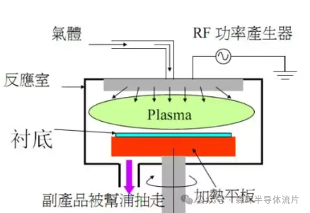
Etch
刻蚀
Removing unwanted materials from the wafer surface using plasma or chemical solutions to form trenches or holes.
Dry etching: Plasma etching (e.g., CF₄/O₂ mixed gas), used for high aspect ratio structures (e.g., TSV, FinFET fins), requiring an etching selectivity of > 10:1 (for Si/SiO₂).
Wet etching: HF solution removes SiO₂, used for surface cleaning or sacrificial layer removal, but with lower precision (μm level).
Depo
沉积
Growing thin film materials on the wafer surface, such as gate oxide layers and interconnect metal layers.
CVD (Chemical Vapor Deposition): Used for insulating layers (SiO₂), semiconductor layers (polysilicon), such as PECVD (Plasma Enhanced) which can deposit high-quality films at low temperatures.
PVD (Physical Vapor Deposition): Sputtering deposition of metal layers (Al, Cu), used for RDL redistribution layers or bump UBM layers.
RTA
快速热退火
High-temperature treatment of wafers for milliseconds (usually > 1000℃), activating dopant atoms and repairing ion implantation damage.
Overlay
套刻精度
The size of the smallest structure on the chip, such as the width of the transistor gate, is a key parameter that determines chip performance. Real-time calibration through the laser interference measurement system of the lithography machine, with error control within 1-2nm.
WAT
Wafer Acceptance Test
晶圆验收测试
Electrical testing of wafers before shipment, verifying whether key parameters (such as threshold voltage, leakage current, contact resistance) meet standards.
Killer Defect
致命缺陷
The size of the smallest structure on the chip, such as the width of the transistor gate, is a key parameter that determines chip performance.
Cycle Time
周期时间
The total time from wafer submission to shipment, usually 90-120 days, with advanced processes (such as 5nm) possibly exceeding 150 days.
MPW
Multi-Project Wafer
多项目晶圆
Multiple designs share the same wafer fabrication, reducing single project costs, suitable for startups or R&D stages.
CP
Chip Probing
晶圆测试
The size of the smallest structure on the chip, such as the width of the transistor gate, is a key parameter that determines chip performance.
Yield
良率
The percentage of qualified chips out of the total production, a core indicator of process maturity.
PPM
Parts Per Million
百万分缺陷率
The number of defective products per million chips, a strict measure of quality.
FinFET
鳍式场效应晶体管
Turning the channel of planar transistors upright to form fins, with the gate surrounding the fins on three sides, enhancing control over the channel.
FOUP
Front-Opening Unified Pod
晶圆传送盒
The size of the smallest structure on the chip, such as the width of the transistor gate, is a key parameter that determines chip performance.
GAA
Gate-All-Around
环绕栅极
The size of the smallest structure on the chip, such as the width of the transistor gate, is a key parameter that determines chip performance.