Table of Contents
CH.1 “Yield” in the Semiconductor Industry
CH.2 Categories of Semiconductor “Yield”
CH.3 Components of Yield
CH.4 Reasons for Low EDS Yield
CH.5 Characteristics of Different Yields
CH.6 Methods for Analyzing Poor Yield
CH.7 EMMI Analysis in Electrical Failure Analysis
CH.8 Why Yield is Important★Important★
CH.9 Solutions for Improving Productivity
CH10. The Relationship Between Yield Improvement and Productivity
CH11. Process Control
CH12. The Importance of Process Control
CH13. Current Issues in Process Control
CH14. Future Trends in Process Control
CH15. Next-Generation Process Control Technologies
Qualcomm’s 3nm Application Processor (AP) manufacturing is entirely entrusted to TSMC instead of Samsung Electronics.
Qualcomm is one of the most important clients for Samsung Electronics. Having the world’s leading fabless giant as a customer is a significant competitive advantage.
However, recent reports indicate that Qualcomm has entrusted all of its 3nm AP manufacturing processes to TSMC. Even the previously fully commissioned 4nm manufacturing process with Samsung will now be split with TSMC, and there are plans to increase orders for 7nm RF chips. The fundamental reason for this is the “yield issue”.
• Qualcomm, the world’s leading fabless company, has decided to entrust all of its next-generation 3nm AP chip manufacturing to TSMC for release next year. Additionally, some of the 4nm AP manufacturing currently done by Samsung will also be transferred to TSMC.
• This decision by Qualcomm stems from Samsung’s low yield in advanced processes, which has led to an inability to guarantee supply capacity. Previously, NVIDIA, the absolute leader in graphics processing semiconductors, also shifted its 7nm graphics card chip manufacturing from Samsung to TSMC. With the loss of major clients like Qualcomm and NVIDIA, Samsung’s foundry business is facing its biggest crisis.
• Reports indicate that the yield of Qualcomm’s 4nm AP chips produced by Samsung is only about 35%; the yield of the Exynos 2200 on the same production line is even below 20%. Therefore, even if Qualcomm wants to give more orders to Samsung, it has to give up due to yield issues.
• Qualcomm, alongside Apple, is considered a “super customer” in the foundry industry, with a massive scale of production. The foundry of high-end products is often a symbol of technological strength. Therefore, in advanced process nodes below 4nm, the competition between Samsung and TSMC will face a greater gap. After Apple, Samsung has also handed over one of its largest customers, Qualcomm’s 3nm foundry orders, to TSMC.
CH.1 “Yield” in the Semiconductor Industry
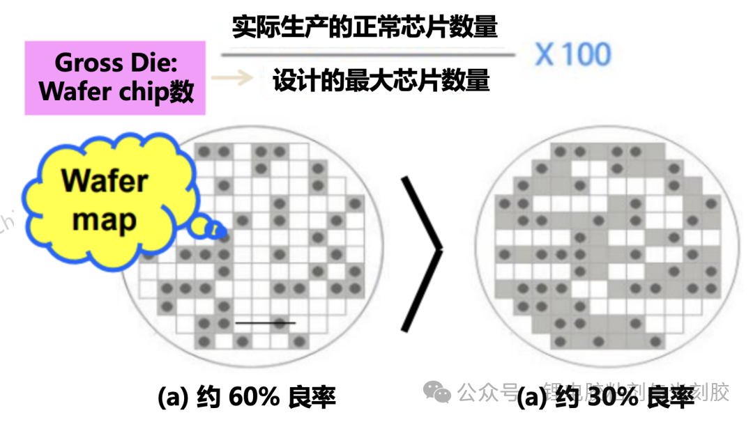
In semiconductors, yield refers to the proportion of defect-free qualified products. It is expressed as a percentage by comparing the maximum number of IC chips designed on a wafer with the actual number of chips that function normally during production. In other words, yield is the ratio of the input quantity to the final output of qualified products.
The higher the yield, the higher the production efficiency, and the company’s sales and profits will also increase accordingly. Therefore, improving yield is extremely important in the semiconductor industry. Since semiconductors are composed of fine circuits, any defect or problem in the manufacturing process can have a fatal impact on the product.
Thus, to achieve high yield, it is necessary to have high-precision process equipment, a clean and dust-free environment, and stable and reliable process conditions, among other guarantees.
CH.2 Categories of Semiconductor “Yield”
Semiconductor yield can mainly be divided into Fab yield, EDS yield, assembly yield, and Final Test yield.
• Fab yield: Represents the ratio of the number of wafers input to the number of wafers output.
• EDS yield: Represents the proportion of functioning chips among the total number of chips. In the semiconductor industry, the term “yield” usually refers to EDS yield. The more chips deemed normal in EDS testing, the greater the contribution to profit.
• Assembly yield: Represents the proportion of all chips that can be normally packaged/assembled.
• Final Test yield: Refers to the proportion of chips that meet normal operation and specification requirements among all assembled chips.
CH.3 Components of Yield
In the semiconductor industry, “yield” typically refers to EDS yield.
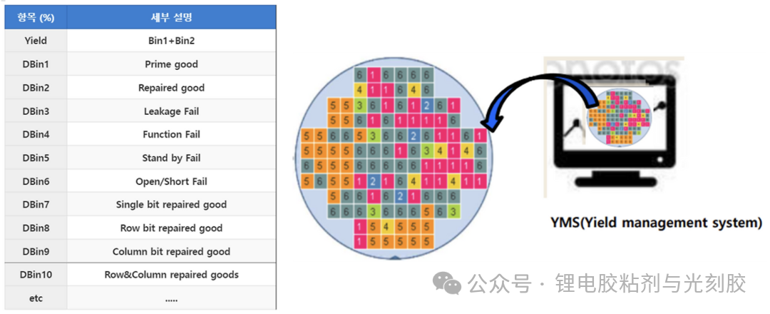
In the Yield Management System (YMS), yield is extracted through Wafer Map, Bin data, and the electrical characteristics of chips, and various statistical analysis methods are used for analysis.
Among them, Bin Code refers to the code used to classify chips based on their status after testing each chip with EDS testing equipment on the wafer after the process is completed.
• Chips with good yield are usually classified as Bin1 + Bin2.
• The remaining chips are classified as Fail chips.
Since EDS yield accounts for the highest proportion of overall value, companies will concentrate all resources and capabilities to maximize EDS yield.
CH.4 Reasons for Low EDS Yield
In semiconductor yield, the reasons for low EDS yield can be roughly divided into parametric failures, systematic failures, and random failures:
• Parametric Failures:
These are the most critical for yield improvement and have localized characteristics on the wafer. They are extremely sensitive to process fluctuations, and testing conditions can significantly affect yield. Most of the time, the causes stem from design defects or insufficient device performance, commonly seen in the early stages of new products.
• Systematic Failures:
These are mostly related to insufficient process margins and are process-related issues. The failure areas tend to recur and are usually more apparent during the initial mass production phase of the product.
• Random Failures:
These occur due to particles within the equipment or defects generated during the process, leading to random failures of chips on the wafer. Generally, this is a topic that needs to be resolved during the mature stage of the product lifecycle (PLC).
Therefore, the order of improvement for yield enhancement is usually: parametric failures → systematic failures → random failures.
CH.5 Characteristics of Different Yields
Abnormal handling process: Abnormal discovery (on-site) → Cause analysis (technical) → Determination (process) → Final approval (quality).
• Fab Yield:
This generally maintains a high yield, indicating almost no fluctuations. Defects caused by process issues, equipment problems leading to broken rejects, and damage during transportation can negatively impact yield.
• EDS Yield:
This has the greatest impact on losses and profits, with many variables affecting yield from R&D to mass production, leading to the largest fluctuations in yield. It is extremely sensitive to design, process, and equipment.
• Assembly Yield:
The yield variation is almost negligible. However, in cases of early design changes, environmental factors, or material issues, defects may occur.
• Final Test Yield:
The goal during mass production is to maintain a high yield. It can also be affected by design changes, process, or material changes. Assembled chips need to undergo performance and functionality testing and are classified into different Bin Codes based on quality levels.
Defective wafers or chips generated during mass production will go through an abnormal handling process and will ultimately be scrapped or rejected.
CH.6 Methods for Analyzing Poor Yield
The yield analysis methods I know include correlation analysis, electrical failure analysis, and physical failure analysis.
Correlation analysis typically utilizes big data analysis to find influencing factors by analyzing the correlation between good or defective wafers and process inputs/outputs, data, equipment, materials, process time, and other elements.
Electrical failure analysis is a non-destructive analysis method that measures TEG components arranged on the wafer scribe lane. This involves measuring physical quantities such as resistance, current, and capacitance for analysis.
Physical failure analysis is a destructive analysis. For wafers, it can detect scope defects; for chips and packages, defects are detected after decapping. Additionally, electrical analysis is combined to confirm defect locations, and various equipment such as SEM, TEM, and FIB are used to analyze defect factors.
Failure analysis plays an important role in semiconductor manufacturing operations, and it also utilizes equipment analysis systems to analyze data related to temperature, pressure, and other wafer manufacturing environment factors.
CH.7 EMMI Analysis in Electrical Failure Analysis
EMMI stands for Emission Microscope, which locates defects by detecting abnormal heat and light.
EMMI is divided into three types: PHEMOS, which analyzes through light emission; THEMOS, which analyzes through thermal emission; and OBIRCH, which detects through resistance changes.
These methods are mainly used to detect defects related to the gate and are also used in detecting metal-related defects.
CH.8 Why Yield is Important★Important★
Semiconductor yield directly relates to a company’s profits. The higher the yield, the higher the production efficiency, and the more revenue the company can generate.
However, more importantly, yield directly relates to trust between the company and its customers. If the yield is too low, it can lead to issues in the chip manufacturing processes required by customers, severely impacting product supply, time to market, and other aspects.
Therefore, yield is both a core competitive advantage among wafer foundries and a commitment to customers. For this reason, process engineers must always devote all their energy to yield improvement efforts.
CH.9 Solutions for Improving Productivity
In the semiconductor industry, there are many factors for improving productivity. First and foremost is yield improvement. The more good dies on each wafer, the more directly it correlates with company profits, making it a critical factor.
Additionally, one example of improving productivity is using larger wafer sizes. Currently, 12-inch (300mm) wafers have become the main process. If larger wafers can be used while maintaining high yield, it can significantly enhance productivity.
Next is the miniaturization of device processes. For example, in DRAM, if the layout area of ITR-IC is reduced from 8F² to 6F² (CD, critical dimension), it can reduce the cell area by 25%, thereby increasing integration. Furthermore, introducing automation systems to increase output per unit time can also enhance productivity.
CH10. The Relationship Between Yield Improvement and Productivity
In the semiconductor industry, the best solution for improving productivity is to enhance yield. Yield improvement leads to an increase in the number of good dies, which directly affects sales. It can also save costs on wafers, chemicals, gases, and other raw materials.
Moreover, yield improvement can reduce labor costs, power consumption, equipment operating time, and other manufacturing costs, leading to an overall increase in productivity. Therefore, yield improvement has become a core issue in the semiconductor industry.
CH11. Process Control
Process control refers to the regular inspection of defects and failures during the semiconductor manufacturing process and measuring whether the processes are manufactured according to the expected design. Since defects in the process can affect product development and production, the role of process control is to appropriately detect and control these defects. Process control can be divided into Inspection, Metrology, and Review. Inspection mainly discovers defects, Metrology measures parameters such as line width and alignment in circuits, and Review provides a more detailed analysis of defects.
CH12. The Importance of Process Control
I really like a saying: “If you cannot measure, you cannot manage; if you cannot manage, you cannot improve.”
Process control plays an extremely important role in improving semiconductor yield. As the complexity of semiconductor processes and the enormous operating costs increase, the ability to achieve timely mass production yield is related to billions of dollars in sales and profit generation. Therefore, process control is crucial.
Currently, with the arrival of the AI era driven by new computing architectures and semiconductor designs, if we cannot continuously promote the development of semiconductor technology roadmaps that support large-scale high-performance logic and memory devices, the costs will be very high. The success or failure of mass production of new semiconductor chips depends on the ability to discover and repair defects. Therefore, process control technologies that can meet new challenges are in critical demand.
CH13. Current Issues in Process Control
Current process control mainly faces three major challenges.
First, semiconductor process technology and device structures are becoming increasingly complex. Traditional optical defect detection methods do not face significant issues in simple patterns that do not require consideration of line width shrinkage. However, today, even extremely small particles can lead to fatal yield defects, making traditional methods often no longer applicable. Current processes involve 3D structures, multiple exposures, and highly repetitive steps, where even slight deviations can trigger unknown fatal defects.
Second, rising costs. As the number of process steps required for each wafer increases, the costs of advanced optical detection systems have also risen significantly. The complexity of processes and the increase in steps mean that more inspections are needed. At the same time, to conduct defect detection, optical scanning equipment has become increasingly precise, which directly raises equipment prices. The increased cost of a scanner ultimately translates into higher costs per wafer scan, significantly increasing overall costs.
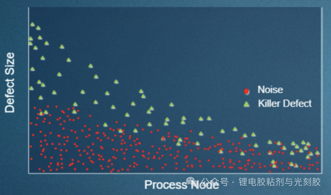
Finally, the most challenging issue is noise. In recent years, the sensitivity of optical detection systems has significantly increased. For example, a 12-inch wafer may generate a wafer map containing millions of potential defects. However, most of these are not actual defects affecting yield but rather ordinary defects that do not impact yield. Semiconductor engineers cannot confirm these massive potential defects one by one, so they usually rely on filtering algorithms to sift through and obtain a controllable dataset.
CH14. Future Trends in Process Control
In the past, minor defects may not have affected yield, but now these minor defects have become factors that reduce yield. As the complexity of semiconductor chips increases, theoretically, more inspections are required, but the current inspection volume has actually decreased compared to the past. Therefore, what the semiconductor industry currently needs is a process control technology that can quickly achieve the required yield in a short time without increasing production costs.
CH15. Next-Generation Process Control Technologies
With the trend of miniaturization, the integration and circuit complexity of semiconductor chips continue to increase, leading to a rising demand for new process control technologies. Current process control technologies are based on big data and AI technologies and are applied in core chip manufacturing processes, forming a new process control system. These technologies can interact in real-time, are faster and more accurate than traditional methods, and can detect and classify defects at a more economical cost.
For example, Company A’s optical wafer detection system combines high resolution with high-speed detection technology, collecting more data during each scan through advanced optical techniques. It is claimed that this economical and efficient optical detection can capture fatal defects while reducing the required costs by three times.
Thus, with the innovation of process control technologies, the overall costs of the semiconductor industry can be effectively reduced, while also providing key technical support for yield improvement.
*If you are satisfied with the content edited by the team, please follow me.
Your attention is my motivation. Thank you*
[Semiconductor Lithography Process] You ask, ChipNote answers: Lithography process and yield-related Q&A 3
[Semiconductor CMP Process] Dishing and Erosion: Invisible Killers in CMP Process
[Semiconductor C&C Process] Semiconductor Flattening from 0 to 1 (Cleaning & CMP) Process
[Semiconductor Etching Process] The Soul of Semiconductors from 0 to 1: Teaching Etching Process and Yield Issues for Engineers
[Semiconductor Lithography Process] You ask, ChipNote answers: Lithography process and yield-related Q&A 2
[Semiconductor Lithography Process] You ask, ChipNote answers: Lithography process and yield-related Q&A 1
[Semiconductor Lithography Materials] i-line vs DUV vs EUV Lithography Resin Key Parameter Comparison
[Semiconductor Process] TSMC 2nm Process and Advanced Packaging
[Semiconductor Lithography Process] Full Process Lithography Optical High NA Principles, DOF, Process Sequence, Resolution, Wavelength, Pre-bake and Post-bake, Introduction to EUV Process
Chip Manufacturing (FAB): Next-Generation Lithography Resin Dry Resist in Semiconductors
[Semiconductor Materials] (Coating, Etching, CMP, Cleaning) New Trends in the Semiconductor Industry Chain: Who’s Opportunity in Materials? Key Processes and Material Introduction
[Semiconductor Lithography Materials] Mask Reticle & Photomask Uses and Production Processes
[Introduction to Semiconductors] Semiconductor Product Development Process from Design to Production (Chip Design Sequence)
[Power Semiconductors] Vertical Structure GaN Power Semiconductor Technology Trends for Electric Vehicle Applications
[Power Semiconductors] Power Semiconductor Discrete Devices and Integrated Circuits
[Mobile Communication Chips] Surface Acoustic Wave Filters for Mobile Communication
[First Communication Chip] 5G Era Innovation: The Rise of Next-Generation RF Chips POI-SAW and TF-SAW, Challenging the Dominance of Traditional SAW/BAW Filters!
[Second Communication Chip] 5G Era Innovation: The Rise of Next-Generation RF Chips POI-SAW and TF-SAW, Challenging the Dominance of Traditional SAW/BAW Filters!
[Display Production] Teaching You How to Use TFT-LCD Production Methods
Chip Manufacturing (FAB): Semiconductor Specialty Gases