Industry Status and Investment Opportunities
The packaging of AI chips primarily utilizes advanced packaging technologies. For instance, NVIDIA’s GPUs consume a significant portion of TSMC’s Cowos, which is a 2.5D packaging technology.
In mainland China, publicly listed packaging and testing companies generally face the issue of being large but not strong. To seize opportunities, we must identify companies that have made breakthroughs in advanced packaging, as only these companies can fully benefit from the dividends brought by AI development.
Core Directions of Technological Development
Let’s first look at the technological development trends in the chip packaging and testing industry. Currently, there are two major directions: the first is wafer-level packaging, which simply means combining multiple identical chips to maximize their utility. The second direction is System-in-Package (SiP), which essentially involves packaging different types of chips together. Chiplet is an evolution of SiP and represents a more advanced form.
-
Wafer-Level Packaging:
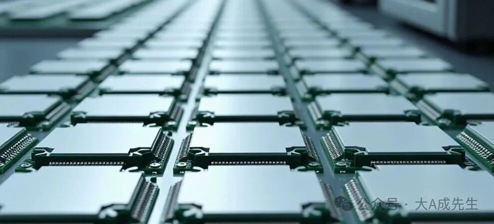
Wafer-level packaging is designed to accommodate more pins within a smaller packaging area by implementing packaging processes directly on the wafer. Traditional chip manufacturing processes involve cutting the silicon wafer into individual chips before packaging, whereas wafer-level packaging reverses this process by packaging first and then cutting. This approach achieves greater bandwidth, higher speed and reliability, and lower power consumption. The market size for wafer-level packaging in 2023 is estimated at $18.45 billion, with a projected compound annual growth rate of around 10% from 2024 to 2032.
-
System-in-Package (SiP):
System-in-Package (SiP) can integrate multiple functional die, such as bare chips, processors, sensors, memory, or passive components like resistors, capacitors, inductors, filters, and even micro-electromechanical systems (MEMS) and optical devices within the same package. Does this technology sound familiar? It resembles System-on-Chip (SoC), but they are fundamentally different. An SoC integrates all functions into a single chip, while SiP focuses on the integration of multiple chips or devices. It can package standard chips, bare dies, and even include SoC as one functional module, combined with memory, sensors, and other components to form a complete system.
Chiplet
Chiplet, known in Chinese as 芯粒, is a further advancement based on SiP. It breaks down complex chips into functionally independent, reusable standardized “small chips” that can be integrated through high-speed interconnect technology. In this sense, Chiplet represents a more advanced form of SiP.
The application scenarios for both are different: SiP emphasizes low cost and rapid integration, suitable for consumer electronics, while Chiplet focuses on high-performance computing, benefiting more from the explosion of AI computing power. Additionally, both SiP and SoC are suitable for consumer electronics and other terminal fields, but SoC products are generally considered more high-end than SiP.
Now that we have a general understanding of the two development directions in the packaging and testing industry, achieving these technological directions requires support from more advanced technologies and processes. We also need to understand several important advanced packaging technologies, such as bump technology, RDL (Redistribution Layer) technology, TSV (Through-Silicon Via) technology, FC (Flip Chip) technology, as well as 2.5D and 3D packaging technologies. We will explain each one to enhance understanding.
Bump, RDL, and TSV Technologies
The principle of bump technology is to use bumps on the chip surface to replace wires. Traditionally, chips connect to substrates using wires, but advanced packaging eliminates the need for wires, allowing direct connection between the chip and the substrate. The denser the bumps, the higher the integration, and the greater the technical challenge.
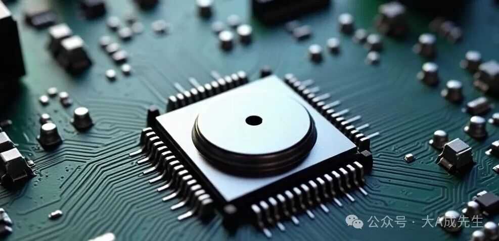
RDL technology is the method for connecting chips horizontally. It involves rearranging input and output ports to a broader area, hence the name redistribution layer technology. Leading overseas manufacturers have achieved line widths and spacings down to 1 micron, while our packaging and testing companies still have some technological gaps.
TSV technology is the method for connecting chips vertically. This is a key technology for achieving 2.5D and 3D packaging. The 2.5D and 3D technologies can be visualized as building a multi-story building where each chip represents a floor, and holes need to be drilled between floors for interconnection, akin to elevator shafts connecting different levels. Currently, TSMC is the only company globally that excels in this technology, and we are not yet at that level, although some companies are making strides in this area.
Flip Chip (FC) Technology
FC technology differs from traditional wire bonding (WB) processes. In traditional processes, chips connect to substrates with metal wires, with the electrical side facing up. The flip chip process involves depositing bumps on the front side of the chip, flipping the chip over, and connecting it to the substrate or frame using the bumps, with the electrical side facing down, hence the name flip chip technology.
This type of packaging offers benefits such as smoother input and output for the chip, reduced interconnection lengths, improved electrical performance, better heat dissipation, and reduced packaging size and weight. Currently, FC packaging holds the largest market share in advanced packaging, with projections indicating that the global FC packaging market will exceed $20 billion by 2025.
Having covered so much technical content, it may be overwhelming for those with a science background. However, once you fully understand these packaging technologies, you will be better equipped to analyze publicly listed companies in the packaging and testing industry, identifying which companies have stronger technological reserves and which are most likely to achieve breakthroughs. You can also discern which companies’ products will benefit from AI computing power development or from future AI application advancements.
Stay tuned, as we will later explore TSMC’s Cowos to understand 2.5D packaging technology, as well as the market space and industry landscape of the packaging and testing sector. (All data sourced from Tonghuashun)
Risk Warning: This article contains various information and insights, intended solely as a reference for investors in securities investment and not as investment advice. Investors bear the risks and consequences of any investments made based on this information.
Disclaimer: 【Xiangcai Securities Co., Ltd. Shenyang Suihua West Street Securities Business Department – Cheng Wei – Investment Advisor – Registration No.: S0500611010051; The above represents personal views for reference only and should not be used as a basis for trading. Risks are borne by the operator. Investment involves risks; proceed with caution.】

Copyright Notice
Text | Cheng Wei Registration No.: S0500611010051
Material | Data sourced from Wind
Editor | Zhao Shenqi Registration No.: S0500625040003
Images | Sourced from the internet; if there is any infringement, please delete immediately!