Semiconductor Equipment: A Shift in Focus

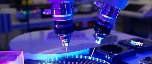
Introduction Etching and thin film deposition are becoming the core areas of market focus. Download for free today: 2025 Semiconductor Industry In-Depth Report Source: Semiconductor Industry Insights Author: Feng Ning Recently, a financial report from Zhongwei Company reflects that the semiconductor equipment market’s focus is expanding beyond photolithography machines to include other core equipment fields … Read more