1. Overview
Xilinx FPGAs starting from the 7 series have on-chip Advanced Encryption Standard (AES) decryption logic, providing a high level of design security. Encrypted Xilinx FPGA designs cannot be copied or reverse-engineered for other FPGAs.The Xilinx FPGA responsible for encryption uses an AES system consisting of software-based bitstream encryption and on-chip bitstream decryption, with encryption keys stored in dedicated on-chip memory. For the 7 series or UltraScale & UltraScale+, the Xilinx Vivado tool can be used to generate encryption keys and encrypted bitstreams; for the Zynq series, the bootgen tool in XilinxSDK/Vitis can be used to generate encryption keys and encrypted package files. Keys can be randomly generated by the tools or specified by the user.Xilinx FPGAs store the encryption keys in dedicated on-chip RAM, which can be optionally stored in BBRAM or eFUSE. For the 7 series, the encryption key can only be programmed onto the device via the JTAG port; the 7 series devices perform the reverse operation, decrypting the incoming bitstream during configuration. The 7 series AES encryption logic uses a 256 bit encryption key. The on-chip AES decryption logic cannot be used for any purpose other than bitstream decryption, and the AES decryption logic is not available for user designs and cannot be used to decrypt data other than the configuration bitstream.The Xilinx 7 series uses the AES-CBC block encryption mode, while the UltraScale & UltraScale+ uses the AES-GCM stream encryption mode, which is more efficient and comes with a GMAC integrity check code to verify the integrity of the ciphertext. The encryption methods and operations are largely similar; this article only introduces the encryption methods for the 7 series and Zynq-7000 bare-metal packaged bin files.
2. 7 Series AES Encryption
2.1 AES
The 7 series FPGA encryption system uses the AES encryption algorithm, which is the official standard supported by the National Institute of Standards and Technology (NIST) and the U.S. Department of Commerce. For specific standards, please refer to: https://csrc.nist.gov/publications/fips/fips197/fips-197.pdf. The 7 series FPGA AES encryption system uses a 256 bit encryption key to encrypt or decrypt 128 bit data blocks at a time. According to NIST, a 256 bit key has 1.1×10 to the power of 77 combinations. Symmetric encryption algorithms ( such as AES) use the same key for both encryption and decryption; therefore, the security of the data relies on the confidentiality of the key.
2.2 Implementation Block Diagram
The Xilinx 7 series encryption and decryption block diagram is shown in Figure 2-1.
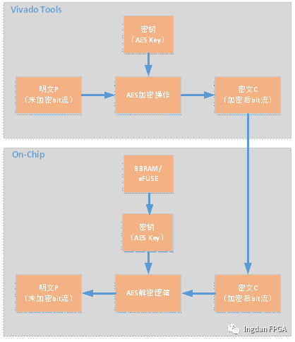
Figure 2-1 Xilinx 7 Series AES Encryption and Decryption Implementation Block Diagram
As shown in Figure 2-1, the Vivado tool is responsible for performing AES encryption on the bitstream based on the user-specified key while writing the key into the dedicated memory on the FPGA; the 7 series decrypts the encrypted bitstream upon loading it, using the on-chip AES decryption logic according to the key set by the user to restore the unencrypted bitstream that the device can recognize.
2.3 AES Implementation Steps
2.3.1 Generate KEY and Encrypted Bitstream
Before this, we need to clarify the differences between BBRAM and eFUSE to facilitate our configuration. The comparison between BBRAM and eFUSE is shown in Table 2-1.
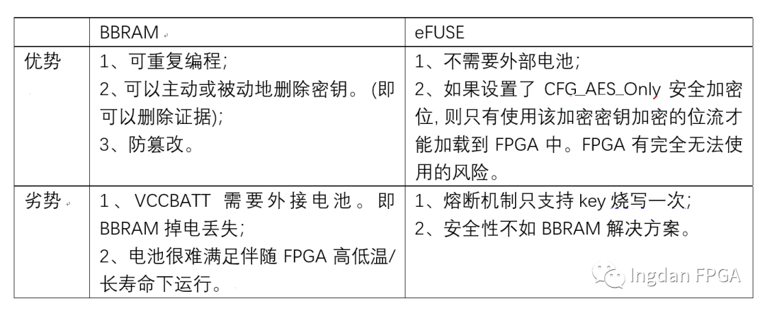
Table 2-1 Comparison between BBRAM and eFUSE
Configure the bitstream properties, select Enable Bitstream Encryption; specify the key storage method (BBRAM or eFUSE); provide the HMAC key, AES key, and the initial vector for AES. As shown in Figure 2-2:
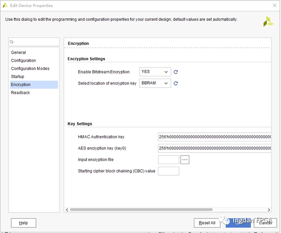
Figure 2-2 Bitstream Configuration Interface
In addition to configuring through the above GUI, the same purpose can also be achieved by directly writing XDC constraint files.
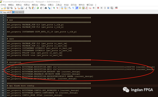
Figure 2-3 XDC Constraint File
If the user does not specify in the GUI or XDC, the tools will randomly generate in the accompanying .key file automatically generated with the bitstream.
The user typically needs to provide three vectors, namely:
A. hkey (HMAC key): The FPGA on-chip supports keyed-Hash Message Authentication Code (HMAC), providing additional security for AES decryption alone. For HMAC, please refer to the specific standard: https://csrc.nist.gov/publications/detail/fips/198/1/final
B. AES key: the 256-bit key (most important).
C. StartCBC: 128-bit AES initial vector.
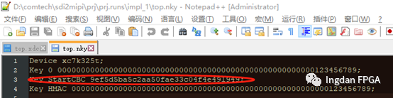
Figure 2-4 Randomly Generated StartCBC in Key File
Once the configuration is complete, the encrypted bitstream can be generated and loaded into the FPGA through JTAG, SPIFLASH, etc. Of course, at this time, the on-chip AES decryption logic does not know the correct key, so the FPGA cannot start normally. The comparison between the encrypted and unencrypted bitstreams is as follows:
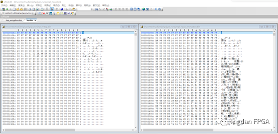
Figure 2-5 Comparison between Encrypted and Unencrypted Bitstreams
2.3.2 Write Key to On-Chip via JTAG
As mentioned earlier, based on the configuration of the bitstream, choose to write the key into BBRAM or eFUSE.
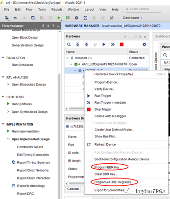
Figure 2-6 Programming Key
Taking BBRAM as an example (if the customer ultimately chooses eFUSE, it is strongly recommended that the user verify first on BBRAM). Select ProgramBBR Key and specify the path to the .key file located in the project bitstream file. The key value is the previously set 256’h123456789. As shown in the figure below:
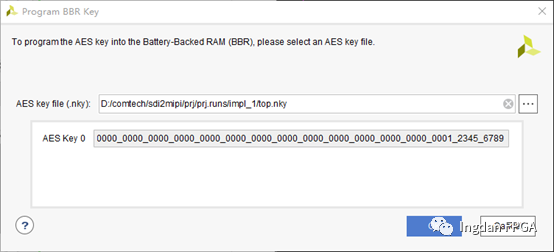
Figure 2-7 Burning Key to BBRAM
Click OK to burn the key to BBRAM, and the Tcl Console will have corresponding prints:

Figure 2-8 Successful Key Burning Print
2.3.3 Verification
Users can try to change the AES key on the vivadobitstream configuration side or the key in on-chip BBRAM for verification, and the program will not load normally.At this time, whether reloading the encrypted program from spi flash or programming the encrypted program via JTAG, the program can be decrypted and executed normally using the AES decryption logic.
2.3.4 eFUSE
eFUSE is a non-volatile one-time programmable technology that is implemented through fuse technology to achieve irreversibility. If access to the register is disabled, that register cannot be re-enabled. FPGA logic can only access the value of the FUSE_USER register. All other eFUSE bits cannot be accessed from FPGA logic.
Therefore, users should be careful when configuring and using eFUSE and pay attention to two points:
A. Ensure that the key is correct and will not be modified again before burning it to eFUSE;
B. Do not modify the values of registers lightly unless you are clear about the true meaning of the eFUSE-related registers. Especially the eFUSE Control Register’s CFG_AES_Only; if this position is set to 1, the on-chip AES decryption operation will be forced, and once the key is forgotten or lost, this FPGA will no longer be usable.
3. ZYNQ-7000 AES Encryption
3.1 Generate Key and Encrypted boot.bin
Similar to the 7 series method, there are two ways to generate the key file:A. Manually edit, modifying the contents according to the above .nky file format, mainly modifying key 0;B. Use the bootgen tool in Vitis or SDK to generate:

Figure 3-1 Content of Key File
Taking the Vitis environment as an example, open a Vitis project and select Xilinx Tools->Create BootImage in the toolbar as shown in Figure 3-2, select the encryption option, and add the files needed for the boot.bin packaging.
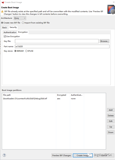
Figure 3-2 Create Boot Image Encryption Interface
Since no key file was specified and the fsbl.elf file was packaged and encrypted, Vitis will automatically generate an .nky encryption file in the directory where the packaged file is generated. The print information during the generation of the encryption file shows the command of bootgen:
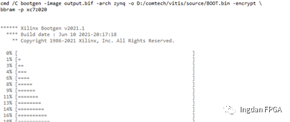
Figure 3-3 Console Print
The generated boot.bin at this time is the encrypted packaged file available for burning.
3.2 Write Key to On-Chip via JTAG
This step is consistent with the operation method of the 7 series; please refer to section 2.3.2.
4. Custom Encryption Using DNA
Xilinx has designed a function with on-chip Advanced Encryption Standard (AES) decryption logic for devices from the 7 series or above, providing a high level of design security. However, there are also some inconveniences for certain customers:A. The BBRAM method requires an external battery to ensure normal operation after power-off restart, and the battery is often difficult to match the FPGA’s lifespan and working environment;B. The fuse mechanism of eFUSE determines that the key can only be burned once and cannot be changed;C. Not friendly for batch production for small customers;D. Older models like Spartan-6 do not support;Based on these reasons, we can use Device DNA (unique ID) to design a custom encryption method suitable for batch production.
4.1 Custom Encryption Flowchart
A custom encryption flow suitable for batch burning is shown in Figure 4-1.
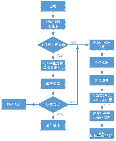
Figure 4-1 Encryption Flowchart
As shown in the figure above, this encryption method needs to utilize the multi-boot feature of Xilinx FPGAs; therefore, there are two copies of the program in the flash, one is the Golden program responsible for encryption operations, and the other is the main program that contains decryption operations. In addition, a space needs to be specified in the flash to store the ciphertext.
4.2 DNA Reading
Each Xilinx FPGA has a unique ID, which is the Device DNA, and it is already hard-coded in the eFUSE register during the production of the FPGA chip, having an unmodifiable attribute due to the use of fuse technology. In the 7 series and earlier devices, the width of the DNA ID is 57 bits; under Xilinx’s Ultrascale architecture, the width of the DNA is 96 bits. The DNA value can be accessed via JTAG, as shown in the figure below:
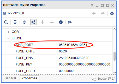
Figure 4-2 JTAG Reading DNA
This design needs to use primitives to read DNA. Taking 7K325T as an example, the primitives and port descriptions are shown in the figure below:
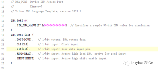
Figure 4-3 DNA Primitives
We only need to design a serial receiving logic to convert the read DNA into 57-bit parallel data, and the read DNA is consistent with the DNA read from JTAG in Figure 4-2.
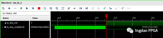
Figure 4-4 Observed Signal for DNA Read with Primitives
4.2 Encryption/Decryption
The encryption/decryption algorithm can use symmetric algorithms such as AES or DES. For models below the 7 series or 7 series, AES or DES encryption/decryption logic needs to be designed independently; for UltraScale & UltraScale+ devices, Xilinx provides AES IP cores that can be applied directly. This article only introduces relatively simple DES encryption/decryption logic.DES stands for Data Encryption Standard, which is a data encryption algorithm successfully researched and publicly published by IBM in 1975. The entry parameters for the DES algorithm are three: key, des_in, mode. Among them, Key is 56 bits and is the working key for the DES algorithm; des_in is 64 bits and is the data to be encrypted or decrypted; mode is the working mode of DES, which has two types: encryption or decryption.
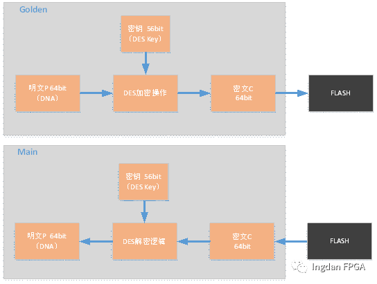
Figure 4-5 Encryption and Decryption Block Diagram
As shown in Figure 4-5, the Golden program in Multi-boot is responsible for extracting DNA as plaintext and performing DES encryption operations with the user-defined key, then writing the encrypted ciphertext into flash. The main program in Multi-boot completes the symmetric mirroring operation, reading the ciphertext from flash and performing DES decryption operations with the user-defined key, then restoring it to plaintext. The following figure verifies the data path through the top-level call of DNA reading, DES encryption, and DES decryption.
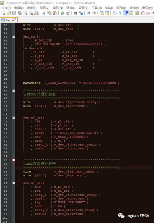
Figure 4-6 Top Level Module Testing
The waveform captured by ILA is shown in the figure below:
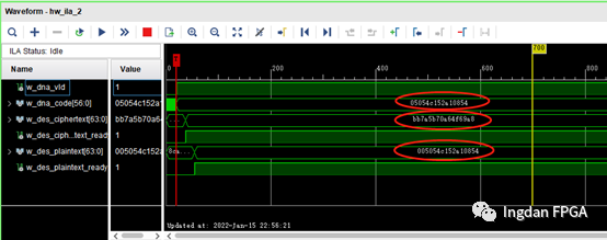
Figure 4-7 Encryption/Decryption Data Waveform
The waveform captured by ILA can verify the symmetry of the DES module.
4.3 Others
In addition to the DNA reading module and encryption/decryption module, a controller for spi flash needs to be designed, which can be implemented via Verilog or through the MicroBlaze soft core. Here, it is recommended to use the MicroBlaze method for design. Specifics will not be elaborated further. The MultiBoot operations involved in encryption can refer to the previous article “Introduction and Implementation of Xilinx FPGA Multiboot Function”. During batch production, a unified MCS file containing Golden and Main is burned into the flash, and then it is attached to each machine. Once powered on, the Golden program will write the ciphertext to flash and self-erase, achieving uniqueness between flash and FPGA to achieve encryption.If you have questions about FPGA encryption, feel free to contact:[email protected][email protected]