Welcome FPGA engineers to join the official WeChat technical group.
Clickthe blue textto follow us at FPGA Home – the best and largest pure FPGA engineer community in China.
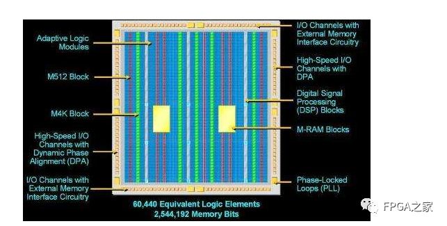
When designing an FPGA, it is often necessary to add constraints during the synthesis and implementation phases to control the synthesis and implementation processes, ensuring that the design meets our required operational speed, pin locations, and other requirements. The usual approach is to write constraint files and import them into the synthesis and implementation tools, guiding the logic mapping and placement and routing during the FPGA/CPLD synthesis and implementation process. Below is a summary of the timing constraint design and analysis for Xilinx FPGAs.
1. Period Constraints
Period constraints are the most common type of timing constraint for Xilinx FPGAs. They are applied to the clock nets, and the timing analysis tools will check whether the timing of all synchronous elements within the clock domain meets the requirements based on the period constraints. Period constraints automatically invert the clock edge of the register. If the clock phases of two adjacent elements are opposite, the delay between them will be limited to half of the period constraint by default.
Before applying period constraints, it is essential to understand the clock period of the circuit to avoid overly loose or tight constraints. Generally, the maximum operational frequency that the designed circuit can achieve depends on the Setup Time and Hold Time of the synchronous elements themselves, as well as the logic and routing delays between synchronous elements. Period constraints are typically defined using the following constraint methods:
1. period_item PERIOD=period {HIGH|LOW} [high_or_low_item]
Where period_item can be either NET or TIMEGRP, representing the clock line name (net name) or the group name (group-name) of the elements. Using NET indicates that the PERIOD constraint applies to the synchronous elements driven by the clock net named “net name”, while TIMEGRP indicates that the PERIOD constraint applies to the group defined by TIMEGRP (including FFS, LATCH, and RAM synchronous elements). period is the target clock period, with units in ps, ns, μS, and ms, etc. HIGH|LOW specifies whether the first pulse in the clock period is high or low, and high or low time specifies the duration of the pulse indicated by HIGH or LOW, with a default unit of ns. If this parameter is omitted, the clock duty cycle is 50%. For example, NET SYS_CLK PERIOD=10 ns HIGH 4ns
2. NET "clock net name" TNM_NET="timing group name";
TIMESPEC "TSidentifier"=PERIOD "TNM reference" period {HIGH | LOW} [high or low item] INPUT_JITTER value;
Often, to define more complex derived relationships of clock periods, this method is used. Here, TIMESPEC acts as an identifier in timing constraints to indicate that this constraint is a timing specification; TSidentifier includes the letter TS and an identifier, together forming a TS attribute; TNM reference specifies which group the timing constraint is applied to, generally added to the group defined by TNM_NET. HIGH | LOW indicates the initial phase of the clock, indicating whether the first clock edge is rising or falling; high or low item refers to the clock duty cycle, which is the time for high or low, defaulting to 1:1; INPUT_JITTER indicates the clock jitter time, within which the clock will jitter, with a default unit of ps. For example, the period constraint:
NET "ex_clk200m_p" TNM_NET = TNM_clk200_p;
TIMESPEC "TS_clk200_p" = PERIOD "TNM_clk200_p" 5.000 ns HIGH 50 %;
This creates a timing group TNM_clk200_p, including all synchronous elements driven by the clock network ex_clk200m_p, all of which will be constrained by the timing specification TS_clk200_p. There is a timing requirement of 5ns between synchronous elements.
2. Offset Constraints
Offset constraints include OFFSET_IN_BEFORE, OFFSET_IN_AFTER, OFFSET_OUT_BEFORE, and OFFSET_OUT_AFTER, which are basic timing constraints that specify the timing relationship between external clocks and data input/output pins, and can only be used with pins. The basic syntax is:
OFFSET = {IN | OUT} "offset_time" [units] {BEFORE | AFTER} "clk_name" [TIMEGRP "group_name"];
Where [IN | OUT] specifies whether the constraint is for input or output, “offset_time” is the time difference between the FPGA pin data change and the valid clock, [BEFORE | AFTER] indicates whether this time difference is before or after the valid clock edge, “clk_name” is the clock name, and [TIMEGRP “group_name”] defines the trigger group for the constraint, defaulting to all triggers driven by clk_name.
1. OFFSET_IN_BEFORE and OFFSET_IN_AFTER constraints
OFFSET_IN_BEFORE and OFFSET_IN_AFTER are both input offset constraints. OFFSET_IN_BEFORE indicates how long before the valid clock edge the input data should be ready. Therefore, the delay of the combinational logic connected to the input pin inside the chip cannot exceed this time; otherwise, data sampling errors will occur. OFFSET_IN_AFTER indicates how long after the valid edge the input data arrives at the chip’s input pin.
The constraint for the internal input logic of the chip with OFFSET_IN_BEFORE is as follows:
NET data_in OFFSET = IN Time BEFORE CLK;
2. OFFSET_OUT_AFTER and OFFSET_OUT_BEFORE constraints
Both of these are output constraints. OFFSET_OUT_AFTER specifies how long after the valid edge the output data stabilizes, and the internal output delay of the chip must be less than this value. OFFSET_OUT_BEFORE indicates how long before the valid clock edge the input data of the next chip should be ready. The delay at the input of the next chip can be used to calculate when the output data of the current design must stabilize. The basic syntax rule is: NET data_out OFFSET=OUT Time AFTER CLK";
3. Specialized Constraints
The general strategy for additional constraints is to first apply global constraints, such as PERIOD, OFFSET, etc., and then apply constraints to local circuits. Specialized constraints include the following:
1. FROM_TO constraints
FROM_TO defines constraints between two groups, controlling the logic and routing delays between them. These two groups can be user-defined or predefined, and can use TNM_NET, TNM, and TIMEGRP to define groups. The syntax is as follows:
TIMESPEC "TSname" = FROM "group1" TO "group2" value;
Where group1 and group2 are the starting and ending points of the path, and value is the delay time, which can be a specific value or expression. For example: TIMESPEC TS_CLK = PERIOD CLK 30ns; TIMESPEC T1_T3 = FROM T1 TO T3 60ns;
2. MAXDELAY constraints
MAXDELAY constraints define the maximum delay of specific network lines, with the syntax as follows:
NET "net_name" MAXDELAY = value units; value is the delay time.
3. MAXSKEW constraints
MAXSKEW is an advanced timing constraint that, when applied to a certain net, can constrain the maximum SKEW on that net. The syntax for MAXSKEW is as follows:
NET "net_name" MAXSKEW = allowable_skew units; For example, NET "Signal" MAXSKEW = 3ns;
4. Group Constraints
In FPGA design, there are often a large number of triggers, registers, and RAM elements. To facilitate adding constraints, they need to be grouped into different categories, and constraints can then be applied to certain groups as needed.
1. TNM constraints.
Using TNM constraints, you can select the elements that constitute a group and assign a name to add constraints. For example: {NET | INST | PIN} "object_name" TNM= "identifier";
Where object_name is the name of the NET, INST, or PIN, and identifier is the group name.
2. TNM_NET constraints
TNM_NET constraints are only applied to nets, and their function is essentially the same as TNM constraints applied to nets, which name all valid synchronous elements along the path of that net. The difference is that TNM is applied to pins, not the synchronous elements along the path of that net, meaning that TNM constraints cannot cross IBUF; using TNM_NET avoids this issue.
NET "net_name" TNM_NET = [predefined_group:] identifier;
TNM_NET can only be used on nets; otherwise, warnings will occur, or the constraint will be ignored.
3. TIMEGRP constraints
Using TIMEGRP constraints, existing group constraints can form new groups, already predefined and defined by TNM/TIMEGRP. TIMEGRP constraints can merge multiple groups into a new group.
TIMEGRP "big_group1" = "small_group" "medium_group"
This merges “small_group” and “medium_group” into a new group big_group1.
5. Simple Methods to Avoid Timing Violations and Remedies
The PERIOD constraint defines the clock period for synchronous elements such as triggers. Timing analyzers can be used to verify whether all paths between synchronous elements meet the design’s setup and hold timing requirements. PERIOD constraint violations will be displayed with negative timing margins in the timing report, indicating whether it is a setup time or hold time requirement violation. One should identify a faster path between the two analyzed synchronous elements. If it is a multi-cycle path, multi-cycle constraints should be sampled, or at least some method should be used to ensure that data arrives in a timely manner and is held long enough for the clock pulse edge to correctly sample it. If the layout and routing software cannot find a faster path, manual routing can be performed using the FPGA Editor tool. However, manual layout and routing are generally not recommended. One should first try restructuring the circuit to meet timing requirements. For example, using a register to introduce a clock can slightly replicate logic, increasing the signal delay but allowing the circuit to correctly sample data.
If the external signal value changes before the clock pulse edge, a DCM or PLL should be used to delay the clock pulse edge so that the data can be correctly sampled by the new delayed clock. An alternative method is to use IDELAY elements in the input/output module to shift the data to a valid clock position.
Generally, increasing the operational speed of the circuit can help minimize timing violations. The specific summary is as follows:
1. By setting Xilinx ISE software in “Implement Design”, right-click to select “Properties”, choose the “Optimization Strategy” column to select “speed”, and right-click to select “Design Goals and Strategies” to choose “Timing performance”.
2. Try to use dedicated resources provided by Xilinx, as FPGA vendors have provided some dedicated resources, such as carry chain MUX, SRL, etc.
3. Reallocate critical paths
(1) Critical paths within the same module can achieve the best timing effects during synthesis.
(2) For critical paths, apply LOC constraints; if the LUTs related to the critical path are too far apart, manual routing using the floorplanner can be employed.
(3) Duplicate circuits to reduce critical path fanout. When the load carried by a signal network increases, its path will also increase accordingly, so duplicating circuits can effectively reduce or even eliminate timing violations.
(4) Insert buffers on critical path networks to reduce fanout, increase speed, and eliminate timing violations.
4. Apply special constraints; setting Multi_Cycle_Path is not very meaningful because it does not directly affect critical paths. This idea is evidently incorrect because it can influence non-critical paths, saving space for critical paths and indirectly achieving the goal of compressing critical path delays, somewhat resembling a “curve to save the country” approach.
5. Modify the code to reduce logic levels and split combinational logic.
Note: Generally, the most frequently used constraints are period constraints; specialized constraints are only needed for certain devices, while high-end FPGAs typically do not require them.

Welcome FPGA engineers and embedded engineers to follow our public account.

National No. 1 FPGA WeChat Technical Group
Welcome everyone to join the national FPGA WeChat technical group, which has tens of thousands of engineers, a group of passionate engineers who help and share with each other, creating a strong technical atmosphere!Hurry up and invite your friends to join!!

Press and hold to join the national FPGA technical group.
FPGA Home Component City
Advantage components service, please contact the group owner: Jin Juan, email: [email protected] Welcome recommendations to procurement
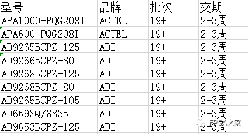
ACTEL, AD part advantage ordering (operating the full series):
XILINX, ALTERA advantage stock or ordering (operating the full series):
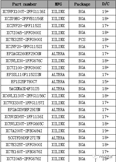
(The above devices are part of the models; for more models, please consult group owner Jin Juan)
Service philosophy: FPGA Home Component City aims to provide engineers with fast and convenient purchasing services for components. After years of dedicated service, our customer service is widespread across large domestic listed companies, military research units, and small and medium-sized enterprises. Our biggest advantage is emphasizing a service-first philosophy, achieving fast delivery, and offering competitive prices!
Directly operated brands: Xilinx, ALTERA, ADI, TI, NXP, ST, E2V, Micron, and more than a hundred component brands, especially skilled in dealing with components subject to US embargoes against China.We welcome engineer friends to recommend us to procurement or consult us directly!We will continue to provide the best service in the industry!

Official thanks to the FPGA technical group brands: Xilinx, Intel (Altera), Microsemi (Actel), Lattice, Vantis, Quicklogic, Lucent, etc.