Welcome FPGA engineers to join the official WeChat technical group.
I originally wrote an introduction to the preliminary debugging plan for high-speed transceivers, providing some initial debugging suggestions when encountering problems. However, I found that it involves many concepts. Explaining them one by one would make the article too lengthy. Therefore, I wrote a separate article introducing the basic concepts, based on Xilinx 7 series GTX.
It should be noted that this text is just a preliminary introduction to the basic concepts, and I will try to use simple and clear descriptions to avoid using technical jargon. I will only describe some basic and commonly used content, and cannot guarantee comprehensiveness. Therefore, from a professional perspective, some terms may differ from the original manufacturer’s documentation, and the coverage may not be enough. Please forgive me.
GTP, GTX, GTH, and GTZ:
These four are the GTs supported by the entire Xilinx 7 series FPGA. GT stands for Gigabyte Transceiver, which is a gigabit transceiver. They are commonly referred to as Serdes, high-speed transceivers, GT, or referred to by specific models (e.g., GTX).
In the 7 series, sorted by the highest line rate supported, GTP is the lowest, and GTZ is the highest. GTP is used in the A7 series, while GTZ is used in a few V7 series. From K7 to V7, the most common are GTX and GTH. The maximum line rate of GTH is slightly higher than that of GTX.
The documentation for GTX and GTH is UG476. From this, it can be seen that the basic structures of these two GTs are quite similar. Therefore, mastering one means you are basically familiar with the other.
UG476 documentation link: https://www.xilinx.com/support/documentation/
TX and RX:
Strictly speaking, TX should be Transmitter, indicating the transmitting part. The structural diagram of the TX part of GTX is shown below:
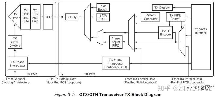
Image from UG476
RX stands for Receiver, and the structural diagram is shown below:
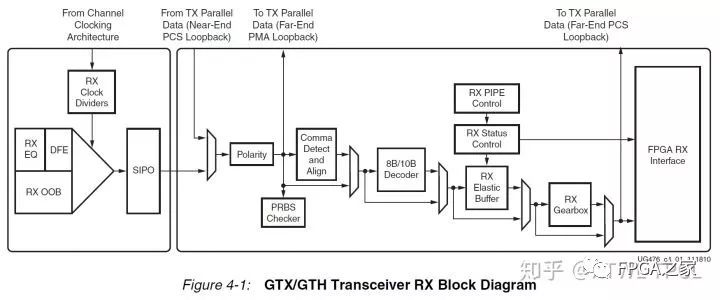
Image from UG476
The following content will use these two diagrams, so you can refer to them.
PMA, PCS
From the structural diagrams of TX and RX, a common point can be seen: the main part of the structural diagram is divided into two parts, a small block diagram on the left and a large block diagram on the right.
The small block diagram on the left is PMA, and the large block diagram on the right is PCS.
To facilitate understanding, the function of PMA can be simply described as:
1. Serial to parallel conversion (SIPO and PISO in the diagram);
2. Analog part;
From this, it can be inferred that the functions within PCS are all parallel digital circuit processing.
Theoretically, the minimum necessary unit of GTX is PMA, mainly due to the core analog part. PCS can theoretically be entirely implemented by the FPGA’s ordinary logic. Of course, the hard-core provided PCS has more functions, better performance, and is more convenient to use.
Elastic Buffer
Commonly referred to as an elastic buffer, its basic structure is a FIFO, often used to handle the cross-clock issues on both sides of the buffer. However, it actually has more uses, such as Clock Correction or Channel Bonding.
There is also a mode that does not use Elastic Buffer, generally referred to as buffer bypass mode, which is considered a high-level application. Interested readers can refer to the documentation for further study.
8b10b
8b10b is usually referred to as a coding method. Here it also refers to a module within the GTX PCS.
As a coding method, 8b10b has balanced levels and prevents consecutive 1s/0s. The encoding is divided into positive and negative codes and special K codes. The most commonly used K code is k28.5. The biggest advantage of 8b10b is its built-in error detection. When an 8b10b error occurs, it is highly likely that there is a problem with the link quality. The biggest disadvantage of 8b10b is its relatively low efficiency, with an extra 20% overhead, so it is commonly used in scenarios below 8G. The most common use of 8b10b, while exceeding 8G line rates, seems to be CPRI Rate 7, with a line rate of about 9.8G.
As a module of GTX, the transmitting end provides a convenient coding interface, and the receiving end provides an easy-to-use output indication, which can be used directly.
Additionally, GTX also provides a Gearbox. Besides 8b10b, there are many other coding methods, such as 64b66b, and the Gearbox is prepared for this type of coding.
PRBS
PRBS stands for Pseudo-Random Binary Sequence. GTX comes with a PRBS generator (inside TX) and a PRBS receiving/checking module (inside RX). The Bit Error Rate (BER) check in ibert is based on the built-in PRBS module.
From the structural diagram, it can be seen that PRBS has no direct relationship with 8b10b, so 8b10b encoding is not used in the ibert test (nor is any other encoding). At the same time, the internal PRBS does not support using other encodings. Therefore, if you want to use a PRBS signal source externally with GTX, you can create a separate PRBS generator and verification module. Xilinx seems to have related reference designs.
ibert
ibert is an IP provided by Xilinx for assisting debugging of GT.
First, clarify that this is an IP. Therefore, ibert has two uses:
1. Directly use the example design for independent use;
2. Integrate it into a project for use;
The two most common uses of ibert are:
1. Bit error rate checking based on the PRBS module;
2. Measuring near-end eye diagrams based on the eye diagram scanning module;
Additionally, ibert allows easy configuration of all parameters of GTX. It is a good parameter testing platform.
Generally, you can try adjusting a few parameters to see if they help the bit error rate/eye diagram of GTX. These parameters are the pre-emphasis of the TX part. The settings for the receiving end are in equalization mode. Since the principle of equalization is quite complex and mostly automatic adjustment, there will not be simple parameters that can show changes.
Distribution of GTX
7 series FPGAs are usually divided by bank. For the GTX banks, they are generally referred to as a Quad, because there are four independent GTX channels in one bank. Each channel is referred to as a Channel. Therefore, in the GTX code, you can see the underlying primitive called Channel.
Each Quad has two reference clock pins and can also obtain reference clocks from the upper and lower Quads (if there are GTX Quads above and below).
QPLL and CPLL
Having known that four GTXs form a group referred to as Quad, and each GTX is referred to as Channel, it is easy to understand QPLL and CPLL. QPLL is a PLL shared by a Quad, and there is only one QPLL for one Quad. CPLL is a PLL unique to each Channel.
From a lower-level perspective, since CPLL is unique to each Channel, all interfaces of CPLL are in the Channel underlying module. QPLL uses another lower-level module called common.
In GTX, QPLL and CPLL differ not only in quantity (one QPLL for a Quad and four CPLLs) and ownership (QPLL belongs to common, CPLL belongs to Channel) but also in the maximum supported line rate frequency. CPLL can only reach a maximum of 6.xG, while QPLL can exceed 10G (specific values need to be checked in the DataSheet according to the device speed grade).
Even if QPLL operates at a very high line rate, the Channel can operate at a lower line rate. The specific implementation scheme is: 1. Use the CPLL that comes with the Channel instead of QPLL; 2. The Channel can reduce the QPLL rate by a factor of 2; thus, under the same reference clock, different GTXs in one Quad have the opportunity to run at different line rates. Of course, this requirement needs more operations, and the IP itself cannot achieve it.
Clock Correction
This function must use Elastic Buffer.
The principle is to specify a key field (similar to the binary number of k28.5), and the transmitting end periodically sends this key field. When the receiving end receives this key field, it checks the position of this field in the FIFO and adjusts it by inserting invalid data/deleting data to keep this field as close to the center of the FIFO as possible, preventing FIFO overflow.
The purpose of this function is to solve the problem of FIFO overflow caused by different clocks.
Channel Bonding
This function must use Elastic Buffer.
The principle is to specify a key field (similar to the number of k28.5). When multiple GTXs receive this field, they will calibrate with each other according to the configuration to ensure synchronized output of parallel data.
The purpose of this function is to perform synchronization processing among multiple GTXs.
GTX IP and Example Design
The GTX IP is the 7 Series FPGAs Transceivers Wizard. It is a very useful tool.
Regarding specific configurations, it needs to be set according to specific applications. Here I will mainly mention two points:
1. Protocol
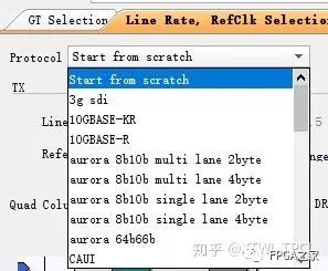
Image from GT IP GUI
In the second tab of the IP configuration interface, there is a Protocol option, usually defaulting to Start from scratch, indicating there are no preset values. Once familiar with GTX and the application requirements, you can use this setting for incremental adjustments. Other options have added some preset values. When unfamiliar with GTX or application requirements, you can first use the preset configuration for learning/testing.
2. Shared Logic
Standalone GTXs usually cannot work directly, and the main reason is the strict reset process of GTX. GTX has a strict reset process. If you design it yourself, it can be time-consuming and labor-intensive. Fortunately, Xilinx provides a reference design – Shared Logic.
Typically, the Example Design is used as the GTX IP for final system integration. The reason for this is that it includes the necessary reset control and other auxiliary designs, making the interface simpler and easier to use. By default, this part is included in the Example Design, and the IP can choose to repackage this part into the IP Core. Thus, the final IP not only has the hard core of GTX but also has a large number of functional modules implemented with ordinary programmable logic, such as Shared Logic.
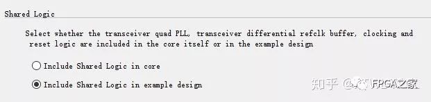
Image from GT IP GUI
After configuring the GTX IP, another very useful function is the Example Design. One advantage of Vivado is that almost all IPs can generate independent and complete Example Designs very conveniently (for example, when needing to use ibert independently).
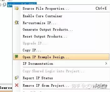
The GTX IP provides source code, with the lowest level being the GTX Channel and common modules. Users can view relevant parameter values and port connections through the code.
GTX’s DRP Port
Generally, an internal module requires reconfiguration using two methods: port control and configuration parameter control.
Port control provides a control port as a switch. For example, in the BRAM port, EN and WE provide high and low levels to change functionality (EN controls whether to use it, WE controls read/write).
Configuration parameter control involves a configuration parameter table, where each parameter has a unique address and corresponding data content. By rewriting the data content at the corresponding address, functionality can be changed.
GTX uses both methods. Therefore, GTX Channel and Common not only have a large number of ports (of course, most ports are functional ports rather than solely for configuration) but also have an address table (refer to the appendix of UG476). Through the DRP port, you can read and write relevant addresses in the address table to obtain data/change configurations.
A common application is line rate switching. In this case, the DRP port is used to adjust some parameter values, and then the GTX is reset to make it operate at different line rates.
Another application of DRP is eye diagram scanning. If you want to scan the eye diagram of GTX, in addition to using ibert, you can also add an eye diagram scanning module to the design for real-time scanning, and this will require the use of the DRP port.
When using the DRP port, one thing to note is the timing of the DRP port. UG476 seems to not provide interface timing. Please refer to the XADC documentation manual – UG480.
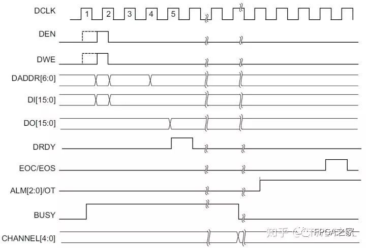
Image from UG480
Loopback
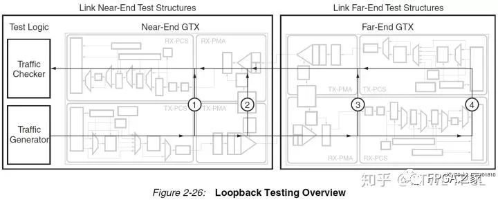
Image from UG476, left is the receiving end, right is the transmitting end
GTX provides four loopback modes, as can be seen from the above figure, the loopback paths are 1, 2, 3, 4.
1 and 2 are near-end loopbacks used for testing the GTX itself. 3 and 4 are far-end loopbacks used for assisting in testing the opposite GTX.
For specific details, please refer to UG476. It should be noted here that the most commonly used is 2, the near-end PMA loopback; the least used is probably 1, the near-end PCS loopback, which basically has no practical effect (think about why). Far-end loopback requires modifying some parameters to use, please refer to the documentation for details.
The introduction to some basic concepts of GTX has been completed. For more details, please refer to the UG476 documentation.

Welcome communication engineers and FPGA engineers to follow our public account.

FPGA WeChat technical group
Welcome everyone to join the national FPGA WeChat technical group, where there is a group of engineers who love technology, and you can discuss technology together!

Press and hold to join the national FPGA technical group.
FPGA technical group platform self-operated:Xilinx Altera Micron, Samsung, Hynix, ADI TI ST NXP and other brand advantages distributors, welcome everyone to send model lists whenever there is a need, and we will provide you with the most competitive quotes as soon as possible!Prices are more than 5% lower than your original supplier! Welcome to inquire – just send your needs to the group owner!
Official thanks to the brands of the FPGA technical group: Xilinx, intel (Altera), microsemi (Actel), Lattice, Vantis, Quicklogic, Lucent, etc.