Welcome FPGA engineers to join the official WeChat technical group.
Clickthe blue textto follow us at FPGA Home – China’s largest and best community for pure FPGA engineers.
This article is mainly to casually record some content related to dedicated clock pins of FPGA encountered while creating constraint files for my current FPGA project, aimed at organizing thoughts, preserving learning results, and providing reference for myself and others in the future.
The reason is that while working on the timing exception constraints in the constraint file, I found that a common timing exception constraint that often appeared in previous FPGA projects of many companies was:

The constraint usually targets the IBUF lines of clock pins brought in externally as communication interfaces like SPI or MDIO, excluding sys_clk.
If this constraint is not added, errors or critical warnings often occur during implementation, and the content will mention that adding this constraint will downgrade severe warnings or errors to ordinary warnings. However, I never understood why this was the case, so I reviewed documents and forums over the past few days to clarify the general idea.
It turns out that there is a class of dedicated clock pins on FPGA pins, which are generally used to bring external clock signals into the FPGA and use these incoming clock signals within the FPGA module. However, if the pin assignment is not done properly during design or if there are not enough pins, there is a possibility that signals that should be connected to dedicated clock pins (also called global clock pins) are instead connected to regular IO pins. This can only be bypassed by adding CLOCK_DEDICETED_ROUTE FALSE to circumvent the PAR check, but it does not solve the fundamental problem.
On the Xilinx 7 series FPGA chips that I often work with, the staff on the Xilinx forum explained this as follows:
If you are bringing the clock onto the device then you need to use the CCIO (Clock capable inputs). Every 7 series FPGA has four clock-capable inputs in each bank. Two of the four are Multi-Region Clock Capable (MRCC) and the other two are Single Region Clock Capable (SRCC). These inputs are regular I/O pins with dedicated connections to internal clock resources.
In other words, it is necessary to use the on-chip MRCC or SRCC pins to bring external clock signals into the FPGA and then use these incoming clocks within the FPGA.
The meanings of these two and their connections are detailed in UG472’s table 1-1:
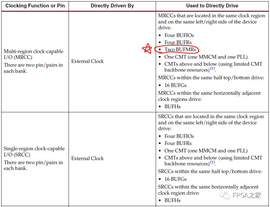
The differences between the two are explained in detail in the answer below on the Xilinx forum at https://forums.xilinx.com/t5/Embedded-Processor-System-Design/MRCC-or-SRCC/m-p/787546:
The clock capable pins in a 7 series FPGA serve two purposes; access to the local clocking resources and access to the global clocking resources.
If you are using the global clocking resources (BUFG, BUFH, MMCM, PLL) then the MRCC and SRCC have exactly the same capability – there is no difference between the two.
If you are using the local clocking resources (BUFR and BUFIO), then the SRCC and MRCC can both only drive the BUFIO and BUFR located in the same clock region. The BUFIO can then only drive the IOB flip-flops and high-speed clock of the ISERDES in the same I/O bank, and the BUFR can clock all the logic (except the high-speed clock of the ISERDES) in the same clock region.
The only difference between the SRCC and MRCC is that the MRCC can also drive the BUFMR. The BUFMR can then drive the BUFIO/BUFR in the same clock region as well as in the clock regions above and below the MRCC. This would generally be used for “ChipSync” (source synchronous) interfaces that need to use more pins than are available in one I/O bank.
Additionally, the answer at https://forums.xilinx.com/t5/Other-FPGA-Architectures/LVDS-CLK-P-N-be-routed-to-MRCC-SRCC-or-regular-differential-IOs/m-p/913220 also mentions:
MRCCs can access multiple clock regions and the global clock tree. MRCCs function the same as SRCCs and can additionally drive multi-clock region buffers (BUFMR) to access up to three clock regions.
Furthermore, the author also mentioned:
If you are forwarding the clock out from the device, then you can use any regular IOs, i.e.
Clock path is
Clock you want to forward -> ODDR -> OBUFDS -> Routed to any regular differential pair.
This means that if you need to bring an external clock into the FPGA but will not use this signal as a clock inside the FPGA module, and only relay or forward this incoming clock, then you do not need to connect it to MRCC/SRCC pins (although these two types of pins can also be used as regular IOs when not used for clock input), and you can connect it to any regular IO instead.
It is also noted that if doing clock relaying, the scheme selected is ODDR-OBUFDS, which is explained in the UG471 document.
UG471-P128:
Clock Forwarding Output DDR can forward a copy of the clock to the output. This is useful for propagating a clock and DDR data with identical delays, and for multiple clock generation, where every clock load has a unique clock driver. This is accomplished by tying the D1 input of the ODDR primitive High, and the D2 input Low. Xilinx recommends using this scheme to forward clocks from the FPGA logic to the output pins.
Additionally, in UG472’s table 2-1, the connection methods of various BUF types after clock input in different application scenarios are explained, including various common clk buffers:
clock management tiles (CMT)
Global clock buffers (BUFGCTRL, simplified as BUFG throughout this user guide). BUFGs do not belong to a clock region and can reach any clocking point on the device.
horizontal clock buffer (BUFH/BUFHCE)
clock enable circuit (BUFHCE)
I/O clock buffer (BUFIO)
regional clock buffer (BUFR)
multi-clock region buffers (BUFMR)
Furthermore, in a blog post at https://www.eefocus.com/liu1teng/blog/12-02/237897_4533d.html, it is mentioned that: If the input-output clock is connected to a regular IO on the hardware, it can be a bit tragic, as it can be connected to the global clock network using BUFG, but there is an inherent delay of 10ns from PAD to BUFG output.This 10ns cannot be eliminated, so if the clock frequency exceeds about 20M, the skew will be relatively large.
This blog post is from 2012 and is somewhat outdated, so the delay data regarding BUFG seems a bit incredible now, and intuitively feels too large, although the author’s 10ns data includes the entire delay from pad-IBUFG (which could be IBUFG or others)-BUFG. I checked the ds181 manual of the Xilinx 7 series FPGA chips currently in use, and found the delay of BUFG in the section on Clock Buffers and Networks, as shown in the following figure:
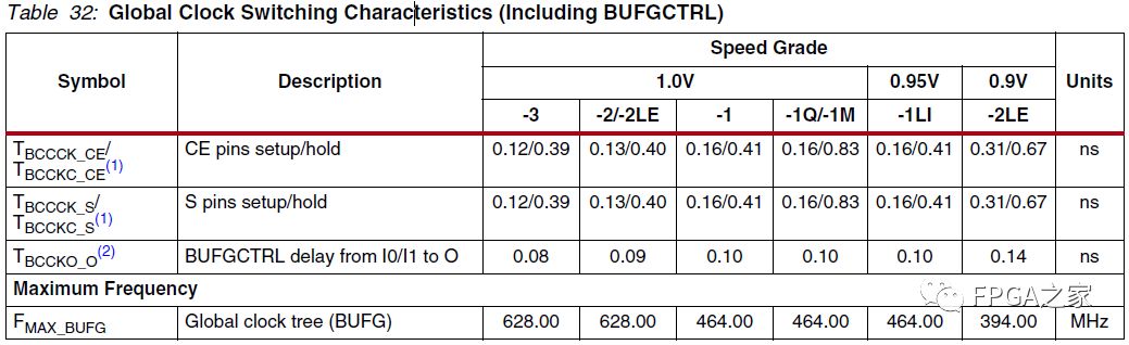
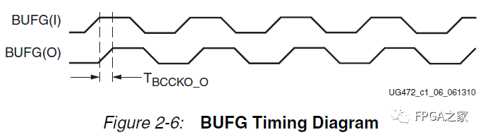
Depending on the speed grade of the chip, this delay varies, approximately around 0.1ns. The Tbccko_o here corresponds to the input-output delay of BUFG in UG472-Figure 2-6, as shown in the following figure:
Additionally, the blog post also mentions:
Some solutions: use two DCMs in series to adjust the phase BUFG+DCM+DCM.
In the current 7 series FPGA, this is equivalent to using clock BUFG+MMCM to achieve clock phase adjustment.
Regarding the development history and differences of DCM, MMCM, and PLL, in addition to referring to UG472, there is a detailed explanation in the response on the Xilinx forum at https://forums.xilinx.com/t5/Welcome-Join/DCM-MMCM-and-PLL/m-p/654372:
The DCM is a Digital Clock Manager – at its heart it is a Delay Locked Loop. This has the ability to deskew a clock, generate different phases of the clock, dynamically change the phase of a clock, generate related (2x) clocks, do clock division, and even generate clocks with harmonic relationships to the incoming clock. It was the only clock management block that existed in older technologies (up to Spartan-3 and Virtex-4).
In Virtex-5 and Spartan-6 the Phase Locked Loop (PLL) was introduced along with the DCM. The PLL is an analog clock management cell that can do almost everything the DCM can do with the exception of dynamic and fine phase shifting. However, it can do more precise frequency generation and can generate multiple different frequencies at the same time. It also has significantly better jitter performance than the DCM – particularly when doing frequency synthesis with large multipliers/dividers.
In Virtex-6 the MMCM – Mixed Mode Clock Manager – was introduced. This is a PLL with some small part of a DCM tacked on to do fine phase shifting (that’s why its mixed mode – the PLL is analog, but the phase shift is digital). Thus the MMCM can do everything the PLL can do plus the phase shifting from the DCM. The V6 only had MMCMs.
In the 7 series, they have a combination of PLLs and MMCMs. Mostly this is so that there are more cells available for use (the PLLs are smaller, so they take less room on the FPGA die). Furthermore, the PLLs are tightly bound to the I/O structures that are used for DDRx-SDRAM memory controllers (via the MIG).
As for the number of them, that is determined by the size of the device. Look at the Product Table for the device you are using – it will tell you what is in the CMT (Clock Management Tile) and how many of them are available in your device.

Welcome communication engineers and FPGA engineers to follow our public account.

China’s largest FPGA WeChat technical group
Welcome everyone to join the national FPGA WeChat technical group. This group has tens of thousands of engineers, a community of engineers who love technology, where FPGA engineers help each other, share knowledge, and have a strong technical atmosphere!Hurry up and invite your friends to join!!

Press and hold to join the national FPGA technical group.
FPGA Home Component City
Advantageous component services, please scan the code to contact the group owner: Jin Juan Email: [email protected] Welcome to recommend to procurement.
ACTEL, AD part of advantageous ordering (full series operation):
XILINX, ALTERA advantageous stock or ordering (full series operation):
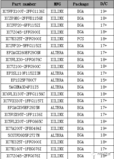
(The above devices are partial models, for more models please consult the group owner Jin Juan)
Service concept: FPGA Home Components self-operated city, aims to facilitate engineers to quickly and conveniently purchase components. After years of dedicated service, our customer service is spread across large listed companies, military research units, and small and medium enterprises. Our greatest advantage is emphasizing the service-first concept and achieving fast delivery and favorable prices!
Directly operated brands: Xilinx, ALTERA, ADI, TI, NXP, ST, E2V, and hundreds of other component brands, especially good at handling components subject to embargoes from Europe and the United States.We welcome engineer friends to recommend us to procurement or consult us personally!We will continue to provide the best service in the industry!

Official thanks to brands in the FPGA technical group: Xilinx, intel (Altera), microsemi (Actel), LattIC e, Vantis, Quicklogic, Lucent, etc.