Welcome FPGA engineers to join the official WeChat technical group.
Clickthe blue textto follow us at FPGA Home – the largest and best FPGA pure engineer community in China.

Introduction: Transmission lines define and control characteristic impedance along their length. However, the three-dimensional structure at their interfaces does not have easily defined or constant impedance along the signal path. To calculate the impedance seen by a 10Gb/s signal passing through these structures, software tools such as 3D field solvers are required, while 2D field solvers are sufficient for calculating transmission line characteristic impedance. PCB designers can use the analyses and examples in this chapter to assist in designing such channels. Cases not covered in this chapter may require further simulation and analysis.
1. Redundant Capacitance and Inductance
Most differential transitions occur through capacitance. The P and N paths are mutually coupled, increasing capacitance. Many transitions have the same frequency response as lumped capacitance over a wide frequency range. By design, increasing inductance can offset this excess.By design, in many cases, increasing inductance can eliminate this excess capacitance, aside from being influenced by density and physical constraints. Techniques such as blind vias, larger pitch solder balls, and very small via pads reduce capacitance, but they are not always feasible in designs.Time Domain Reflectometry (TDR) technology, whether through simulation or measurement, allows designers to identify redundant capacitance or inductance during the transition process.
2. Time Domain Reflectometry (TDR)
To perform TDR measurements, a step input is applied to the interconnect. By observing the reflected signal, the location and magnitude of the redundant capacitance or inductance experienced by the voltage step as it traverses the interconnect can be determined.Parallel capacitance (see Figure 1) causes an instantaneous drop in impedance, while series inductance (see Figure 2) causes an opposite direction impedance discontinuity. Td is the propagation delay through the first transmission line segment on the left. The reflected wave generated by the impedance discontinuity requires 2*Td to return to the TDR port. If the propagation speed of the signal through the transmission line is known, the location of redundant capacitance or inductance along the channel can be calculated.
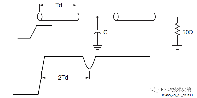
Figure 1, TDR characteristics of parallel capacitance
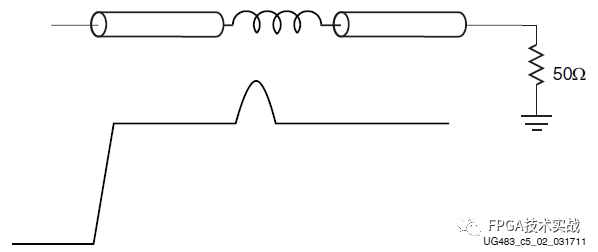
Figure 2, TDR characteristics of series inductanceThe size of this redundant capacitance (C) or inductance (L) can also be extracted from the normalized area of the integral of the TDR of the step transition. The corresponding equations for reactive capacitance and inductance are:
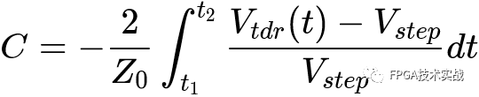 (Equation 1)
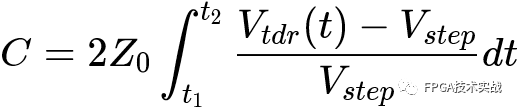 (Equation 2)
Figure 3 shows the integral of the normalized TDR area.
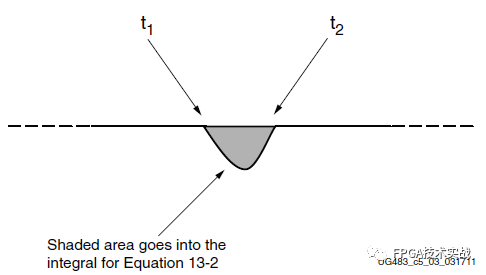
Figure 3, Integral of normalized TDR area
Results obtained using these equations are insensitive to changes in rise time and are valid for simulated TDR measurements, provided that the preceding and following transmission lines are very close to 50Ω. However, for actual measurements, accuracy is highly dependent on Z0.
3. BGA Packaging
Each signal path in BGA packaging is carefully designed to optimize signal integrity. Single-ended I/O routing is typically designed for a 50Ω impedance. Routing for high-speed SERDES I/O is designed for a nominal 100Ω differential impedance. Special care should be taken when designing signal paths to optimize discontinuities, such as solder balls and substrate vias, to minimize their impact on signal integrity. A 3D full-wave electromagnetic solver and vector network analyzer are used to model and measure packaging performance.
4. SMT Pads
For applications requiring AC coupling between transmitters and receivers, SMT pads are introduced into the channel to allow the installation of coupling capacitors. Standard SMT pads have redundant capacitance due to the capacitance of nearby reference planes. In the example shown in Figure 4, a 5 mil trace (Z0 of 50Ω) transitions to a 0402 SMT pad, which is 28 mils wide, all exceeding 3 mils of FR4.
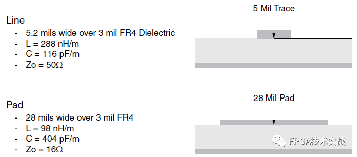
Figure 4, 2D field solver analysis of a 5 mil trace and a 28 mil pad At these dimensions, a 2D field solver shows that the Z0 of the 5 mil trace is 50Ω. The Z0 of the 0402 pad is 16Ω, as the capacitance of the pad is too high and the inductance too low, resulting in an impedance less than 50Ω. The performance of this transition can be optimized in one of two ways. The first method keeps the width of the trace the same as the pad and moves the ground layer deeper in the stackup to maintain the Z0 of the transition segment at 50Ω. This method does not require any special analysis, but the edge capacitance of the surface mount capacitor body will introduce some error. Trace density is limited as the trace is now 28 mils wide. The second method, as shown in Figure 5, clears the ground layer below the pad, thereby eliminating a significant amount of redundant capacitance caused by the board capacitance between the pad and the ground layer. This technique allows for greater trace density than the first method but requires 3D field solver analysis or measurement along with several iterations of the PCB design to achieve the desired performance.
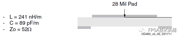
Figure 5, Example of transmission optimization The 2D field solver indicates that if the ground plane beneath the pad trace is cleared, the resistance can approach 50Ω. The result can then be verified more extensively using a 3D field solver. The ground plane shown in Figure 6 is identical to that in the 2D simulation. Using frequency domain analysis in HFSS, this technique can improve return loss by 20dB (10x).
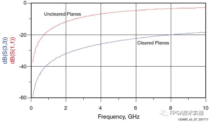
Figure 6, Pad clearance Ansoft HFSS model Figure 7 shows the comparison of return loss between the 0402 pad structure and linear scaling.
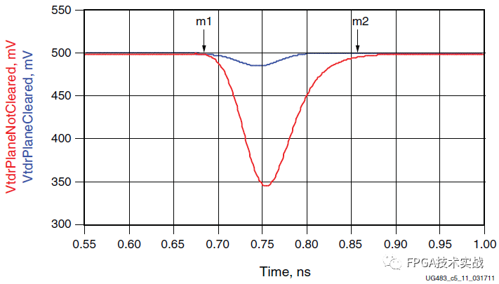
Figure 7, Comparison of return loss of 0402 pad structure The slope of about -40 dB/decade in Figure 8 closely matches the frequency response of the lumped capacitor.
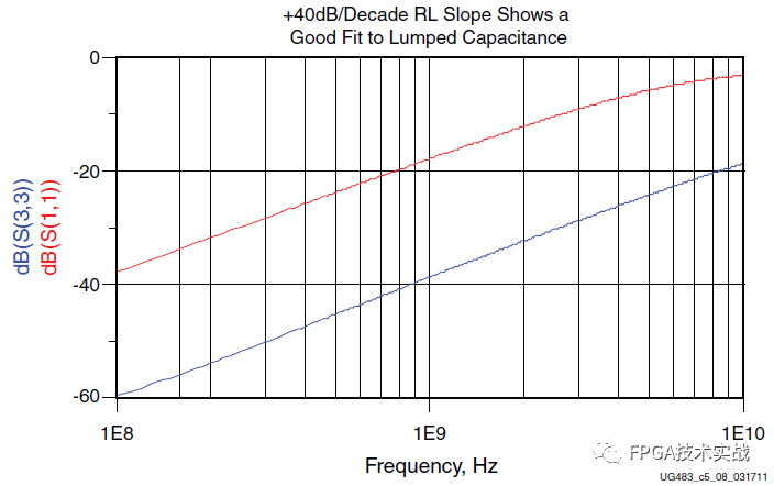
Figure 8, Comparison of return loss of 0402 pad structure on a logarithmic (frequency) scale Next, using the simulated transition in HFSS, the time domain performance of the transition can be measured by performing TDR on the early frequency domain analysis S-parameter results. In Figures 9 and 10, the red curve with a large capacitive tilt corresponds to the SMT pad, which has not had the ground layer cleared from below. The blue curve shows that clearing the ground layer can eliminate most of the excess capacitance.
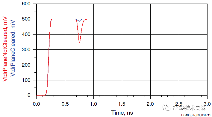
Figure 9, TDR results comparison of 0402 pad structure
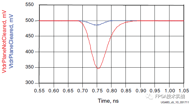
Figure 10, TDR results comparison of 0402 pad structure
Figure 11, Excess capacitance of 840 fF when the ground layer is intact
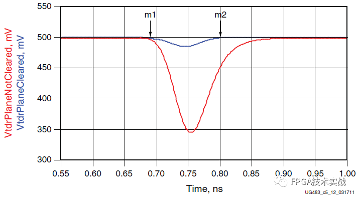
Figure 12, Excess capacitance of 57 fF when the ground layer is intact
5. Differential Vias
The most common transmission is through differential vias, where signal pairs must transition from the upper stripline layer or top microstrip to the lower stripline layer or bottom microstrip. Figure 13 shows a ground-signal-ground-signal (GSSG) type differential via. The ground vias connect to each ground layer in the stackup, while the signal layers only contain pads for the entry and exit layers.
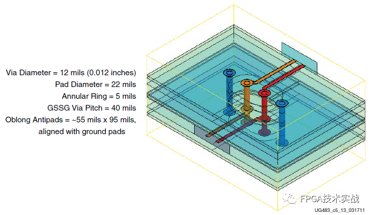
Figure 13, Example of differential via design
The key advantage of GSSG vias is that they allow the return current of the signal to flow in ground vias near the corresponding signal vias, thereby reducing excessive inductance. The signal paths are also symmetric between the P and N halves of the differential signal, which is crucial for controlling common-mode artifacts caused by P/N imbalance.
Larger rectangular solder pads reduce excess edge capacitance between the via body and surrounding plane edges. Unused pads are also removed. A good starting point is to use the dimensions shown in Figure 13 as an example for an 80 mil differential via design. To accommodate density constraints or lack thereof, the dimensions can be scaled accordingly to maintain the ratio of each dimension relative to the others. This scaling maintains the impedance performance of the differential vias while allowing changes in overall size to better fit specific applications. These final dimensions are constrained by manufacturability and density considerations. While via lengths can be slightly altered to accommodate thicker or thinner boards than 80 mil, changing the ratio of via length relative to other dimensions will affect the impedance of the via. For this and other configurations of differential vias, it is best to use 3D field solver tools to simulate the model to ensure performance targets are met.
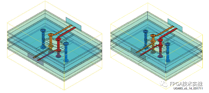
Figure 14, Differential GSSG via in a 16-layer PCB As a general rule, the P and N paths need to maintain equal lengths during transmission. Where possible, the stub lengths of the vias should be kept to a minimum by routing the signal through the entire length of the via. The analysis shown in Figure 15 compares the common-mode (SCC11) and differential (SDD11) response S-parameter return loss.
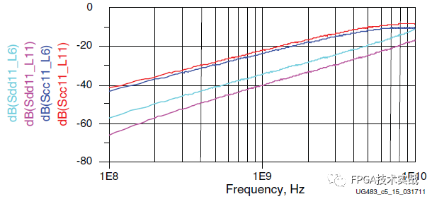
Figure 15, Simulated return loss comparison of GSSG vias L11 and L6
From the chart in Figure 15, the common-mode response is 20 dB worse in terms of return loss. The common-mode response is much poorer compared to the differential response, which is why it is a good idea to minimize P/N deviation as much as possible before entering transmission. The 60/40 rule of thumb indicates a return loss of 40 dB at 1 GHz, which means 60 fF of excess capacitance. Since excess capacitance is a monopole response, simple extrapolation rules can be applied. For example, if the return loss shifts to 34 dB, the excess capacitance will double. Due to the excellent performance of GSSG vias, even long via stubs can at most double the capacitance of the differential via.
6. P/N Cross Vias
Some transceivers provide the ability to independently switch the polarity of the transmit and receive signal pairs. This feature eliminates the need for P/N crossed signals at the board level, significantly enhancing signal integrity. P/N cross vias should be avoided if possible, and the polarity switch of the transceiver should be utilized.
7. SMA Connectors
Well-designed SMA connectors can reduce debugging time and allow high-performance channels to be correctly designed on the first pass. To achieve this performance goal, simulation, design, and manufacturing of shape memory alloy connectors that perform well at 10Gb/s are necessary. Vendors can also provide design services to ensure that connectors work properly on specific boards. Assembly guidelines are critical for ensuring that the matching process between connectors and circuit boards is well controlled to provide specified performance.
Xilinx uses precision SMA connectors manufactured by Rosenberger and other precision connector manufacturers because they offer excellent performance and the points listed in the previous section.
8. Backplane Connectors
Backplane connectors present numerous signal integrity issues, including:
-
P/N signal deviation
-
Crosstalk
- Shorted transmission lines due to connector pins
Some connector manufacturers provide not only specifications, models, and layout guidelines for connectors but also design support, workshops, and tutorials.
9. Microstrip/Stripline Bends
When differential traces pass through a 90° angle, the outer traces are longer than the inner traces, leading to P/N imbalance. Even within a single trace, the signal current tends to hug the inner trace of the corner, further reducing the actual delay through the bend. To minimize the skew between P and N paths, 90° bends in microstrip or stripline are arranged as two 45° bends to provide an angle. Adding a jog out also allows for trace length matching. Figure 16 shows an example of bends in traces.
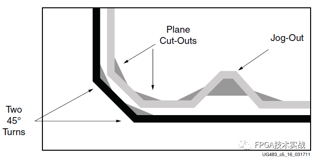
Figure 16, Design example of 90-degree bends in traces The number of turns increases capacitance, as the width of the trace at the 90° angle is 41%. When using a 45° bend, the difference decreases to 8%. Adding plane vias at a depth of 30 mils can reduce excess capacitance. When simulating this angled bend with smoothing cuts and plane cuts, excess capacitance is reduced, improving P/N length and phase matching. Without the jog-out, the P/N length mismatch is 16 mils. Given FR4 material, a 16 mil difference translates to a 4.8° phase mismatch at 5 GHz, or 2.68 ps (0.0268 ui) at 10Gb/s. Figures 17 to 19 show that the phase mismatch is reduced to 0.75° using the smoothers and jog-out, and the phase mismatch is reduced to 0.3°. The simulation results combining smoothing and jog-out indicate that the residual capacitance of the structure is reduced to 65 fF. Designers attempt to widen the traces to compensate for the increased characteristic impedance due to less strong separation and coupling of the traces. However, even without widening the traces, the combined capacitance of the corners and jog-out is still over-capacitive, so the non-coupled portion of the smoothing output cannot be widened.
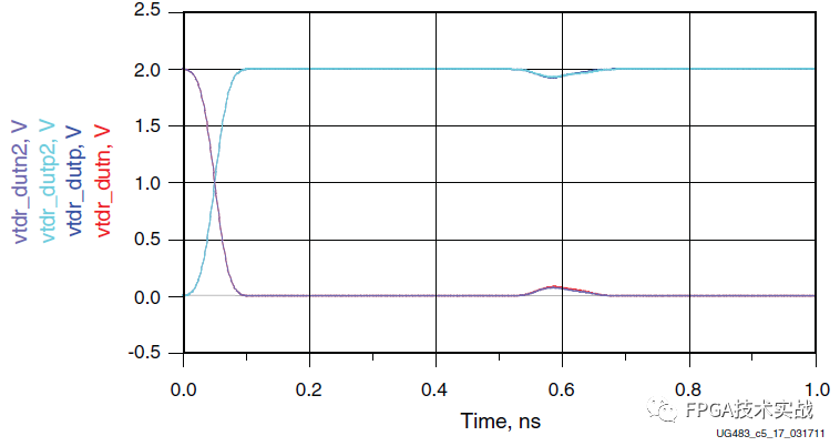
Figure 5-17: Simulation TDR of 45-degree bends with jog-out
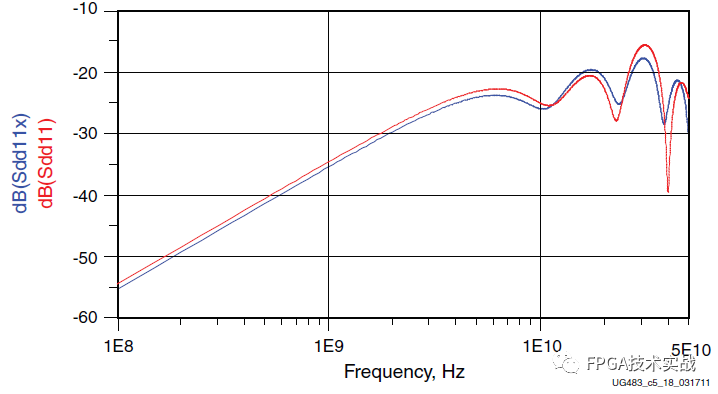
Figure 18, Simulated return loss of 45-degree bends with jog-out
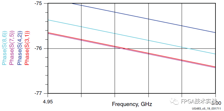
Figure 5-19: Simulated phase response of 45-degree bends with jog-out
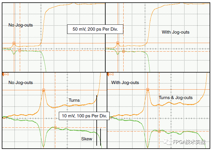
Figure 20, Measured TDR of 45-degree bends, with and without bends
Welcome FPGA, Embedded, Signal Processing engineers to follow the public account

National Largest FPGA WeChat Technical Group
Welcome everyone to join the national FPGA WeChat technical group, which has tens of thousands of engineers, a group of engineers who love technology, helping each other and sharing here, creating a strong technical atmosphere!Hurry up and invite your friends to join!!

Press and hold to join the FPGA national technical group
FPGA Home Component City
Advantaged component services, please scan to contact group owner: Jin Juan Email: [email protected] Welcome to recommend to procurement
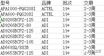
ACTEL, AD part of advantageous ordering (operating the full series):
XILINX, ALTERA advantageous stock or order (operating the full series):
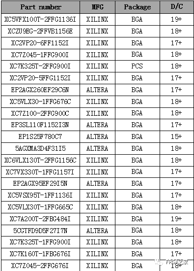
(The above components are part of the models, for more models please consult group owner Jin Juan)
Service philosophy: FPGA Home component self-operated city aims to facilitate engineers to quickly and conveniently purchase components. After years of dedicated service, our customer service is spread across large listed companies, military research units, and small and medium-sized enterprises. Our biggest advantage is emphasizing the service-first philosophy and achieving fast delivery with favorable prices!
Directly operated brands: Xilinx, ALTERA, ADI, TI, NXP, ST, E2V, Micron and over a hundred component brands, especially good at handling components under U.S. embargo against China,Welcome engineer friends to recommend us to procurement or consult us personally!We will continue to provide the best service in the industry!

Official thanks to the FPGA technical group brands: Xilinx, intel (Altera), microsemi (Actel), LattIC e, Vantis, Quicklogic, Lucent, etc.