Q&A | How Texas Instruments Contributes to a Sustainable Future
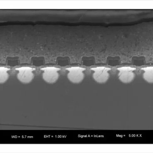
Click the blue text above Follow us! For decades, Texas Instruments has been committed to reducing its environmental impact, setting goals such as improving production efficiency and reducing greenhouse gas emissions, and achieving them one by one. These actions have yielded significant results. Texas Instruments’ “2022 Corporate Citizenship Report” shows that since 2015, we have … Read more