“IT Chat” is a professional IT information and service platform under the Machinery Industry Press, dedicated to helping readers master more professional and practical knowledge and skills in the broad field of IT, quickly enhancing their workplace competitiveness. Click the blue WeChat name to quickly follow us.
This article is reprinted from: Fresh Date Classroom
Author: Little Date Jun
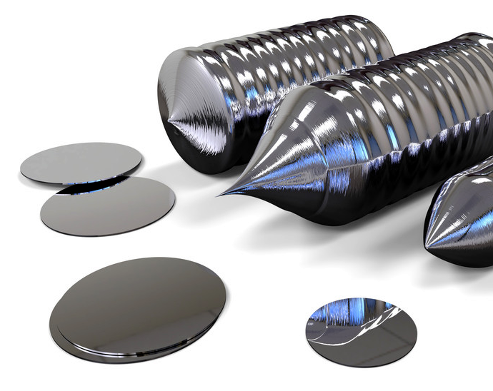
Silicon Ingots and Wafers
Today, we will discuss the manufacturing process of chips (die).
This stage is the most challenging part of the chip manufacturing process. I will try to explain it in a simple and understandable way, and I hope everyone can patiently read through it.
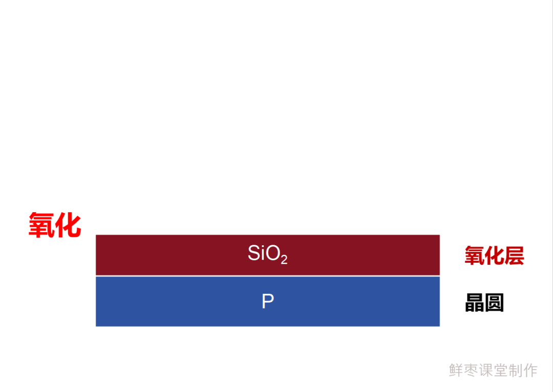
█ Oxidation
First, after cutting and polishing the wafer, we need to perform an oxidation step.
The purpose of oxidation is to form a protective film (oxide layer) on the fragile surface of the wafer. The oxide layer can prevent the wafer from being affected by chemical impurities, leakage currents, and etching.

The oxidation process includes thermal oxidation, plasma-enhanced chemical vapor deposition (PECVD), and electrochemical anodic oxidation.
Among these, the most commonly used is thermal oxidation, which forms a thin and uniform layer of silicon dioxide at high temperatures of 800~1200°C.
Depending on the gases used during oxidation, it can be classified into dry oxidation and wet oxidation.
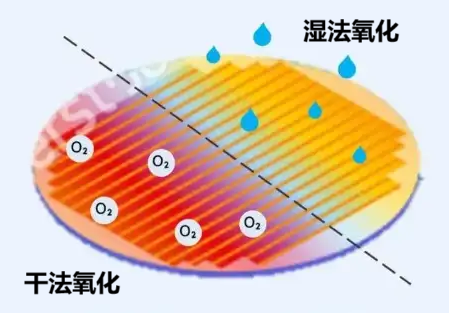
Dry oxidation involves introducing pure oxygen, allowing it to flow over the wafer surface, reacting with silicon to form a silicon dioxide layer. Wet oxidation uses both oxygen and high solubility water vapor.
Dry oxidation is slower but results in a very thin and dense oxide layer. Wet oxidation is faster but results in a relatively thicker and less dense protective layer.
Currently, dry oxidation is the mainstream technology in semiconductor manufacturing. Wet oxidation is more commonly used for non-critical layers or specific thick film requirements.
█ Photolithography (Coating, Pre-bake, Exposure, Post-bake, Development)
Next, we finally arrive at the most important step— photolithography.
For the past few years, we have been concerned about the “bottleneck” photolithography machines, which are related to this step.
Photolithography, in simple terms, is like a printing machine that “etches” the chip circuit diagram onto the wafer.
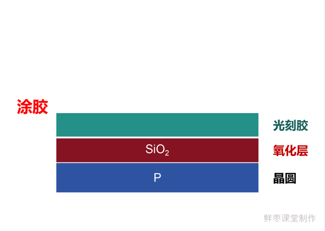
Photolithography can be divided into three main steps: coating, exposure, and development. Let’s look at them one by one.
First, there is coating.
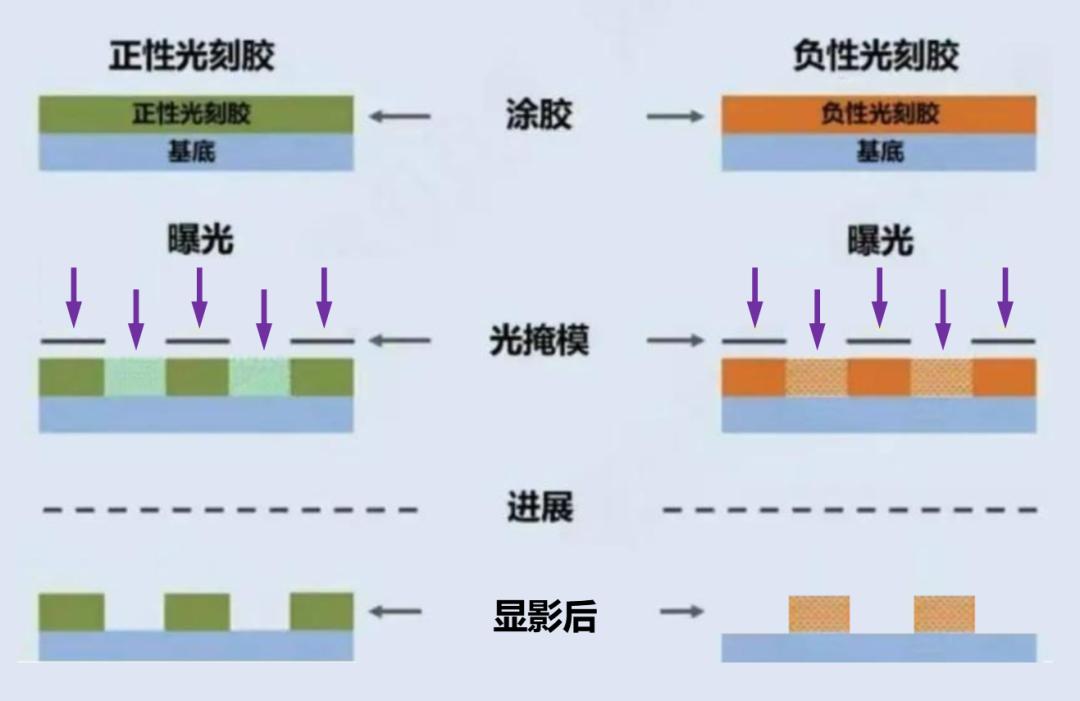
The material used for coating is called photoresist, sometimes also referred to as resist, which is a light-sensitive material.
There are two types of photoresist: positive and negative.
Positive resist, when exposed to a specific light beam, undergoes a change in molecular structure, becoming more soluble. Negative resist, on the other hand, becomes less soluble when exposed. In most cases, positive resist is used.
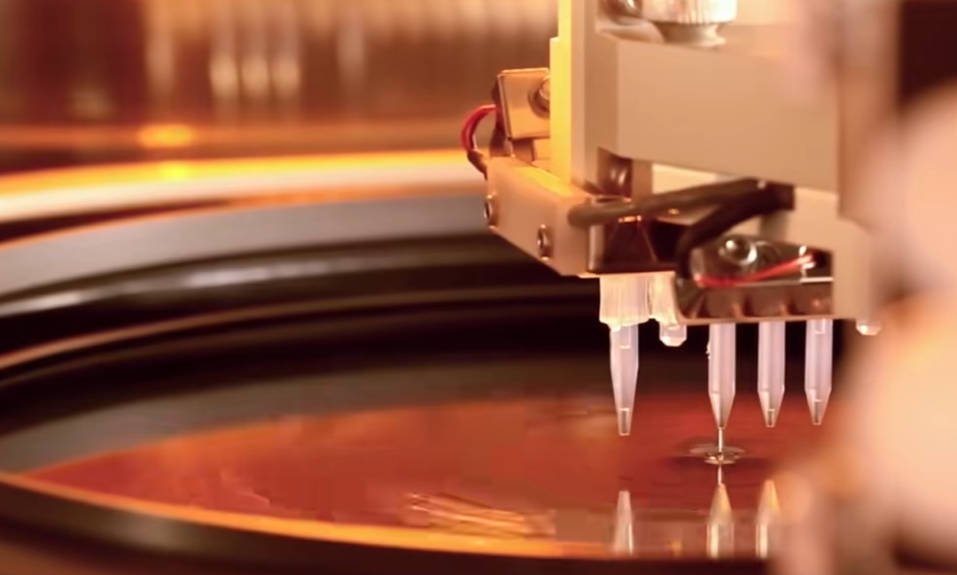
During coating, the wafer is first spun at a speed of 1000~5000 RPM. Then, a small amount of photoresist is poured onto the center of the wafer. The photoresist spreads across the entire surface of the wafer due to centrifugal force, forming a uniform coating layer that is 1 to 200 microns thick.
 Coating
It is worth mentioning that photoresist is also a highly technical material. Most of the photoresist used domestically comes from Japan.
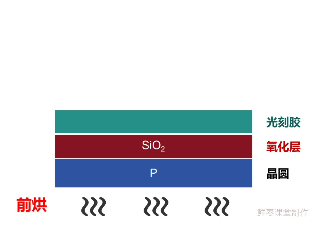
After coating, the wafer undergoes a soft bake to slightly solidify the photoresist. This step is called “pre-bake”.
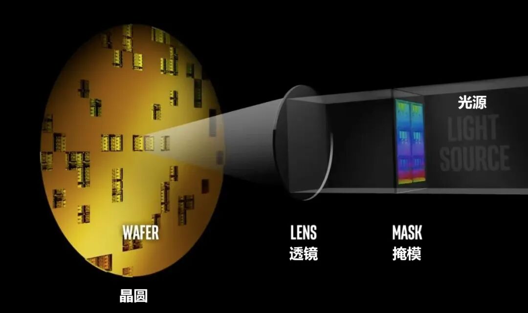
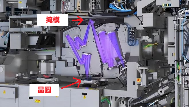
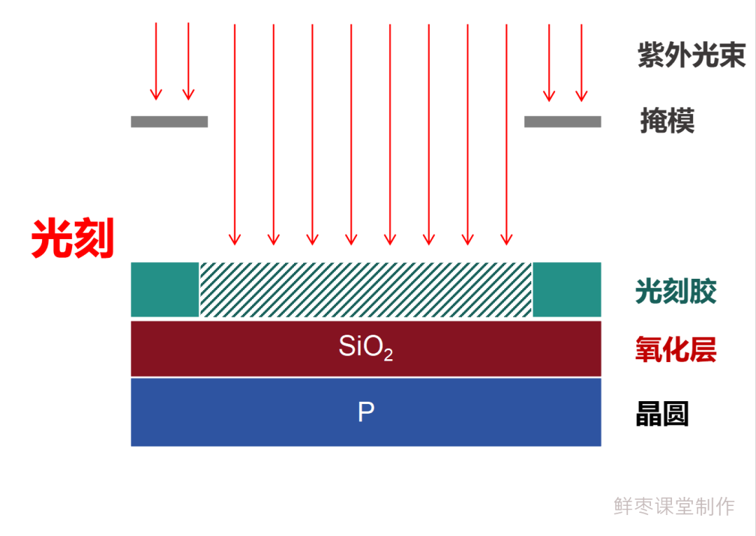
Next, the photolithography machine comes into play for exposure.
The wafer is placed in the photolithography machine, along with the mask.
The mask, formally known as the photolithography mask, is also called a resist, and its English name is mask. It is the core of the photolithography process and an important output of the chip design phase.
The mask is a glass or quartz plate with an opaque material (such as chromium) pattern layer. The pattern on it is actually the blueprint of the chip, which is the integrated circuit layout.
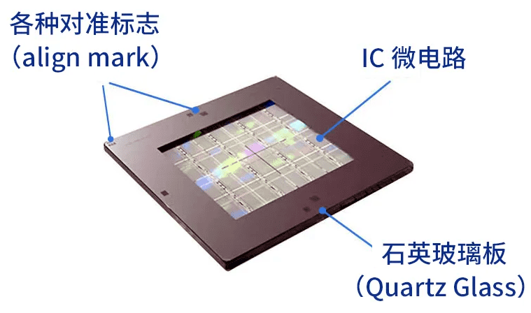
Mask
In the photolithography machine, both the wafer and the mask are precisely fixed. Then, the special light source of the photolithography machine (mercury vapor lamp or excimer laser) emits a beam (ultraviolet light), which passes through the hollow parts of the mask and multiple lenses (to converge the light), ultimately projecting onto a small area of the wafer.
The fine circuit pattern is thus “projected” onto the wafer.
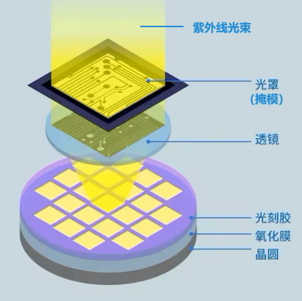
For positive photoresist, the exposed areas become more soluble. The unexposed photoresist remains intact.
The mechanical position fixing the wafer and mask continuously moves, and the beam keeps shining. Ultimately, the circuit “drawing” of dozens to hundreds of chips is completed across the entire wafer.
Photolithography machine working process
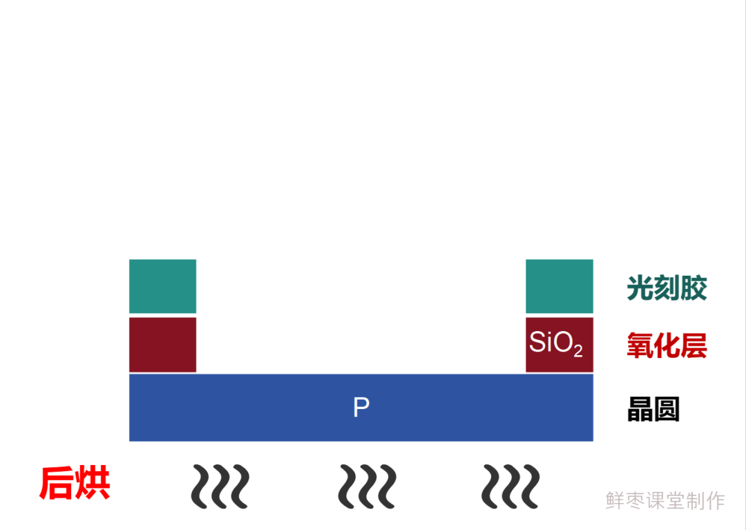
After the wafer comes out of the photolithography machine, it must undergo another heating baking process (baking for 20 minutes at 120~180°C), referred to as post-bake.
The purpose of post-bake is to ensure that the photochemical reactions in the photoresist are fully completed, compensating for any insufficient exposure intensity. At the same time, post-bake can also reduce the concentric rings caused by the standing wave effect after the development of the photoresist.
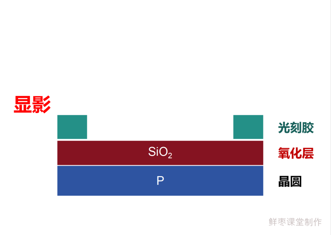
Next is development.
After exposure, the wafer is immersed in a developing solution. The developing solution removes the exposed photoresist (positive resist), revealing the pattern.
Then, the wafer is rinsed and dried, leaving a precise circuit pattern.
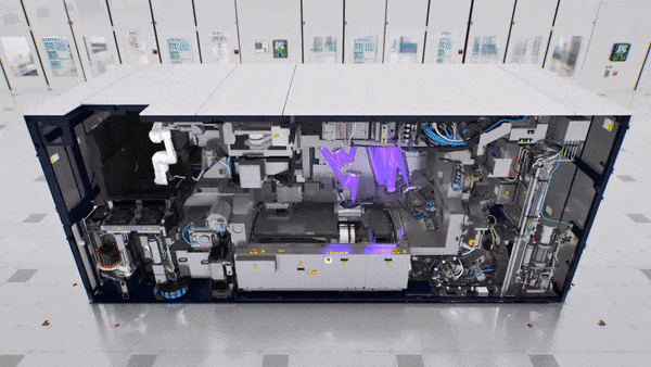
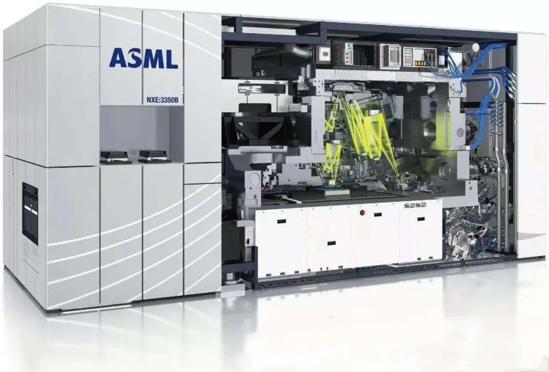
█ About Photolithography Machines
Here, I would like to insert a segment specifically discussing photolithography machines.
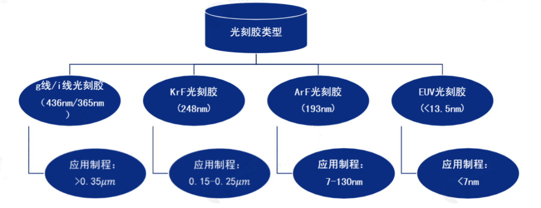
Traditional photolithography technology typically uses deep ultraviolet light (DUV) as the light source, with a wavelength of about 193nm (nanometers). The wavelength of the light wave limits the minimum feature size that can be manufactured in the photolithography process (i.e., the resolution limit). As chip processes continue to evolve, traditional DUV photolithography technology gradually fails to meet the requirements.
Thus, the EUV photolithography machine was developed.
EUV photolithography machines use extreme ultraviolet light (EUV) as the light source, with a wavelength of only 13.5nm, far smaller than DUV. This allows EUV photolithography to create smaller feature sizes, meeting the manufacturing needs of advanced chip processes (such as 7nm, 5nm, 3nm).
EUV photolithography has extremely strict requirements for beam concentration and process precision. For example, the mirrors used for reflection in EUV photolithography have a length of 30cm (centimeters), and the surface undulation must not exceed 0.3nm (nanometers). This is equivalent to requiring that the undulation of a railway track from Beijing to Shanghai not exceed 1mm.
The extremely high technical specifications make the manufacturing of EUV photolithography machines very difficult. There are only a handful of companies worldwide capable of developing and manufacturing EUV photolithography machines. The leading company in this field is the renowned Dutch company ASML.
According to information disclosed by ASML, each EUV photolithography machine contains 100,000 parts, 40,000 bolts, 3,000 wires, and 2 kilometers of hoses. The vast majority of the components in the EUV photolithography machine come from the most advanced products from various countries, such as gratings from the United States, lenses from Germany, bearings from Sweden, and valves from France.
The cost of a single EUV photolithography machine reaches up to 100 million USD, and it weighs 180 tons. Each transport requires 40 containers, 20 trucks, and three flights to complete. Each installation and debugging also takes at least a year.
ASML’s production of EUV photolithography machines is limited to a maximum of 30 units per year, and they are reluctant to sell them to us. The most severe “bottleneck” in the entire chip industry is this EUV photolithography machine.
█ Etching
Alright, let’s continue discussing the chip manufacturing process.
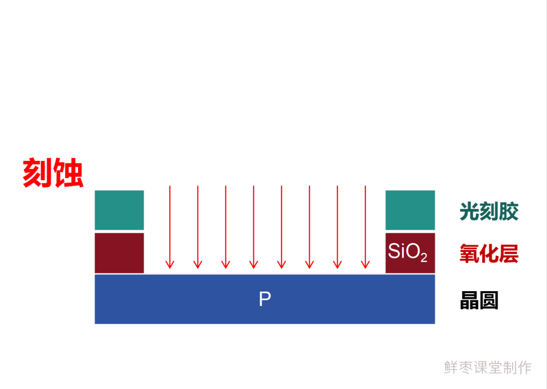
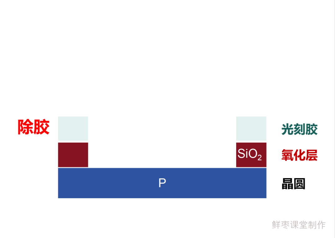
Now, although the pattern has appeared, we have only removed part of the photoresist. What we really need to remove is the underlying oxide layer (the part not protected by the photoresist).
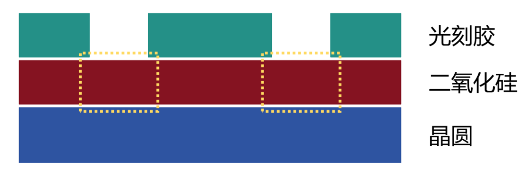
In other words, we need to continue to “dig holes”.
The process to be used at this time is etching.
Etching processes can be divided into wet etching and dry etching.
Wet etching involves immersing the wafer in a liquid solution containing specific chemicals, using chemical reactions to dissolve the semiconductor structures (oxide film) that are not protected by the photoresist.
Dry etching uses plasma or ion beams to bombard the wafer, removing the unprotected semiconductor structures.
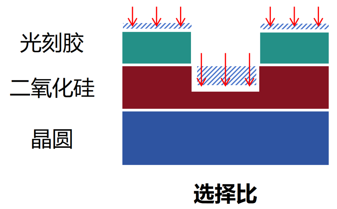
In the etching process, there are two concepts to pay attention to: isotropy (anisotropy) and selectivity.
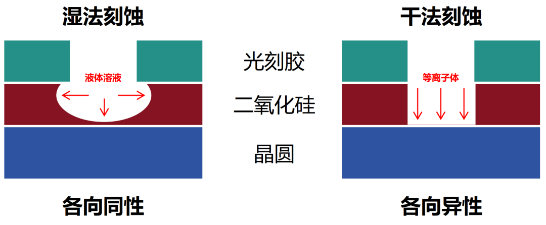
As shown in the figure above, during wet etching, the etching occurs in all directions, which is called “isotropic”. In contrast, dry etching only etches in the vertical direction, which is called “anisotropic”. Clearly, the latter is better.
During etching, both the oxide layer and the photoresist are etched. Under the same etching conditions, the etching rate of the photoresist compared to the etching rate of the material being etched (oxide layer) is called selectivity. Obviously, we want to etch as little photoresist as possible while etching more oxide layer.
Currently, dry etching dominates and is the preferred choice in the industry.
This is because dry etching has stronger fidelity. Wet etching is difficult to control in direction. In advanced processes like 3nm, it can easily lead to reduced line widths or even damage circuits, thereby reducing chip quality.
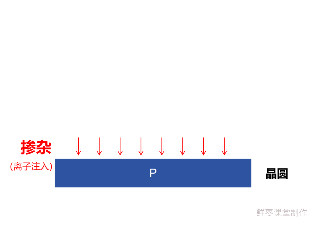
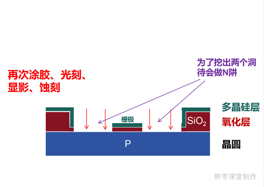
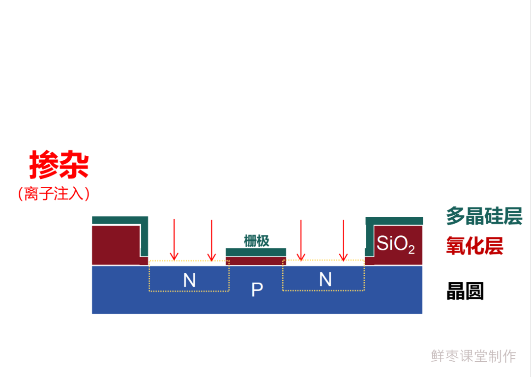
█ Doping (Ion Implantation)
Alright, the “digging holes” process has been introduced.
At this point, the surface of the wafer has been etched with various grooves and patterns.
Next, let’s take a look at the doping process.
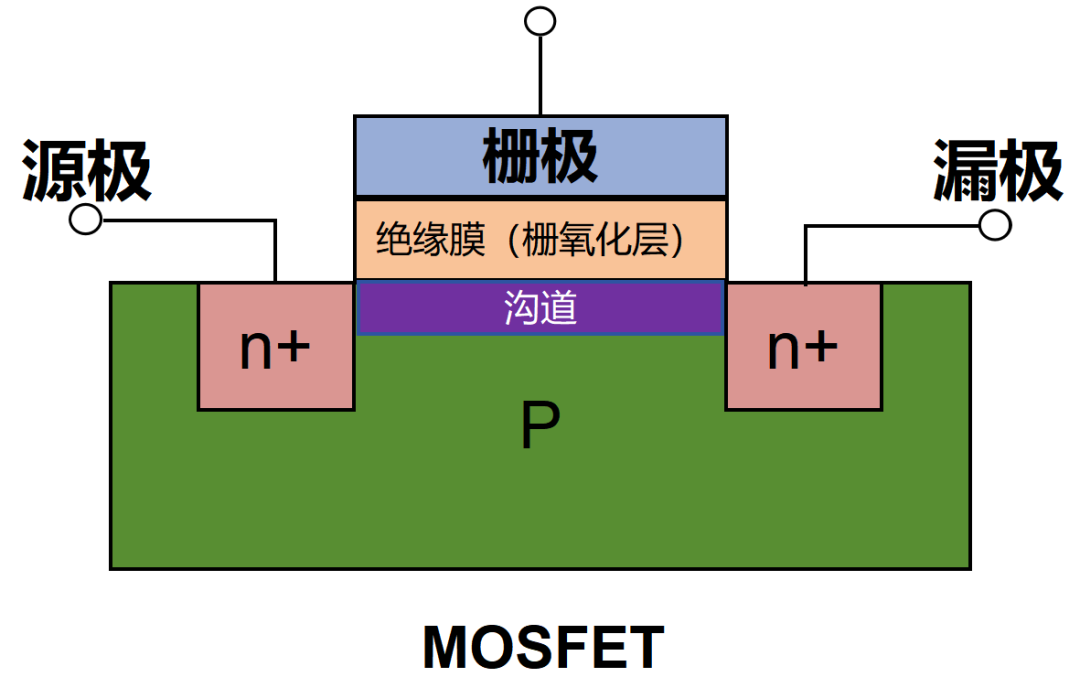
Transistors are the basic building blocks of chips. Each transistor is based on a PN junction. As shown in the figure below (MOSFET transistor, NPN), it includes P wells, N wells, channels, gates, etc.
In the previous photolithography and etching, we only dug holes. Next, we need to construct P wells and N wells based on these holes.
Pure silicon itself is non-conductive. To make non-conductive pure silicon into a semiconductor, we must introduce some impurities (called dopants) into the silicon to change its electrical properties.
For example, introducing phosphorus, antimony, and arsenic into silicon can create N wells. Introducing boron, aluminum, gallium, and indium can create P wells.
N has free electrons. P has many holes and a small number of free electrons. By applying a voltage to the gate on the channel, we can attract electrons from P, forming an electron channel (channel). When voltage is applied to both N, a current is formed between NPN.
As shown in the figure below:
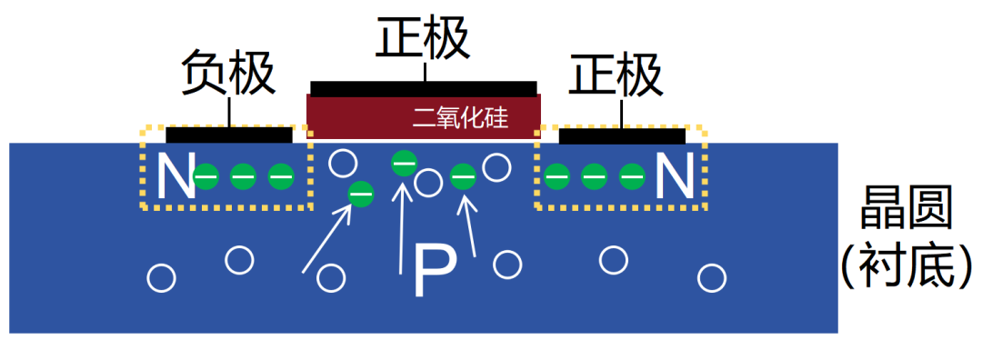
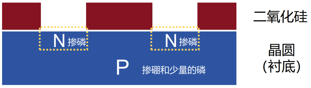
In the figure, the bottom is the P well substrate. The two holes are N wells.
In other words, when making this NPN transistor, ion implantation was already used to dope the substrate with boron (containing a small amount of phosphorus) before the initial oxidation (for ease of reading, I did not mention this step earlier).
Now, the “dug holes” can be doped with phosphorus to become N wells.
Did everyone understand? The purpose of doping is to create PN junctions and transistors.
Doping includes thermal diffusion and ion implantation processes. Due to the difficulty of achieving selective diffusion with thermal diffusion, most processes currently use ion implantation.
Ion implantation involves using high-energy particle beams to directly shoot impurities into the silicon wafer.
The ion source is usually an injection gas (for convenience), such as phosphine (PH3) or boron trifluoride (BF3). As the gas passes through the ionization reaction chamber, it is bombarded by high-speed electrons, causing the electrons of the gas molecules to be knocked off, turning them into ions.
At this point, the ion composition is quite complex, including boron ions, fluorine ions, etc. A mass spectrometer is used to construct a magnetic field to deflect the ions, selecting the required ions (different ions have different deflection angles), which then collide with the wafer to complete ion implantation.
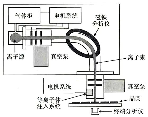
Structure of the ion implantation machine
(Source: “Introduction to Semiconductor Manufacturing Technology”)
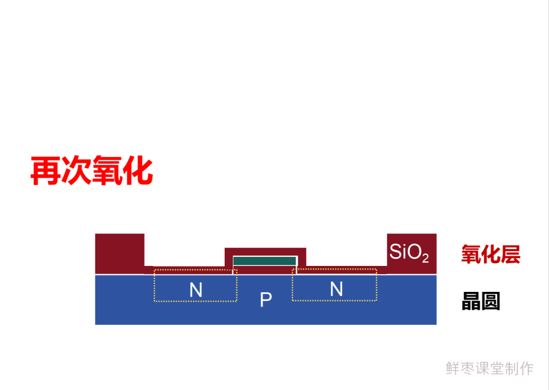
At this point, the silicon dioxide layer (oxide layer) becomes the barrier layer for ion implantation.
After ion implantation, the silicon surface needs to be heated to 900°C for annealing.
Annealing allows the implanted dopant ions to further diffuse uniformly into the silicon wafer. It can also repair the damage caused to the wafer lattice during ion implantation (the lattice of the silicon substrate is damaged during ion implantation).
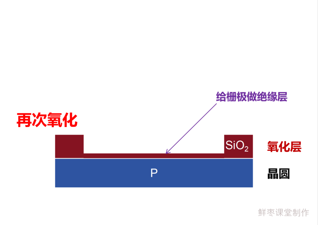
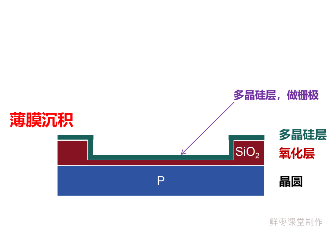
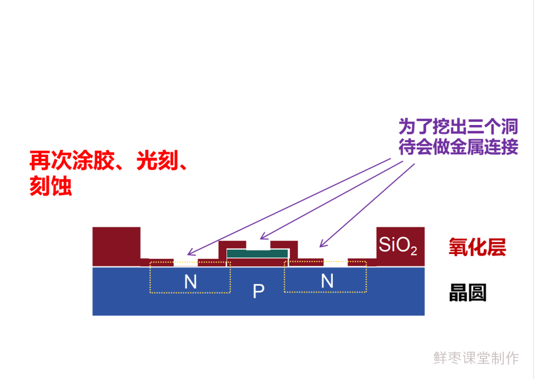
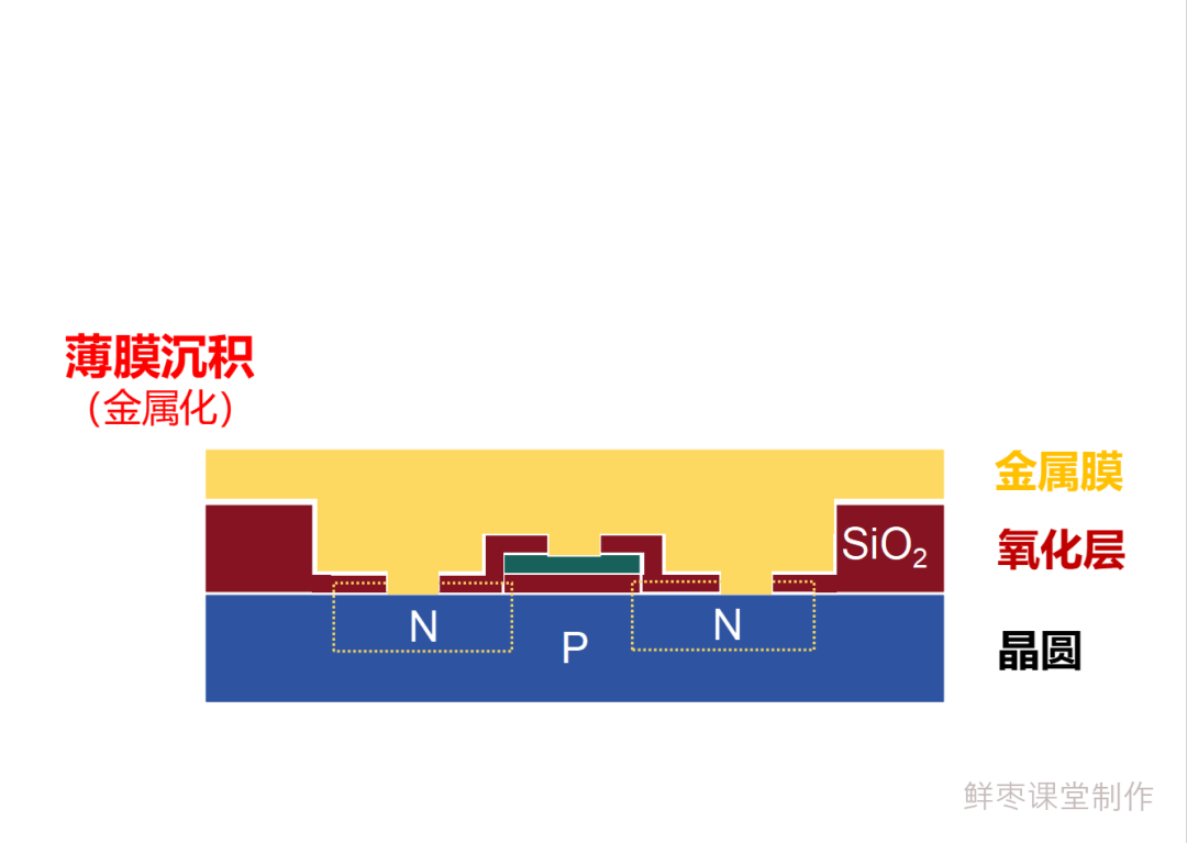
█ Thin Film Deposition
Having discussed so much, we are now at the stage of “building the building”.
Let’s first look at a structural diagram of a finished chip (partial example):
You will find that this is a very complex three-dimensional structure. It has many layers, somewhat like a building, and also resembles a complex three-dimensional traffic network.
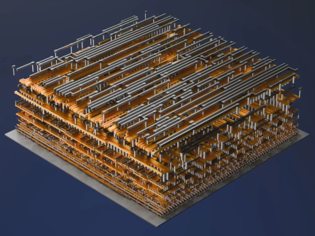
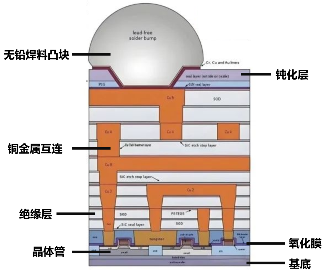
At the very bottom of this structure is the silicon substrate we painstakingly created earlier, which serves as the foundation.
As the base of the chip building, the substrate must have good thermal stability and mechanical properties, and it also needs to provide some electrical isolation to prevent interference.
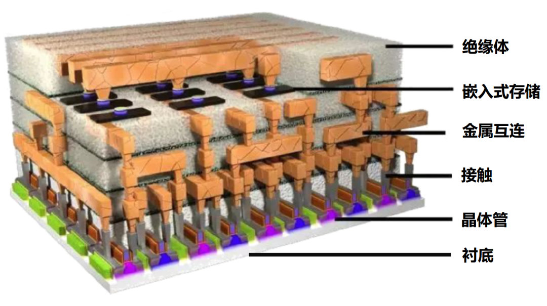
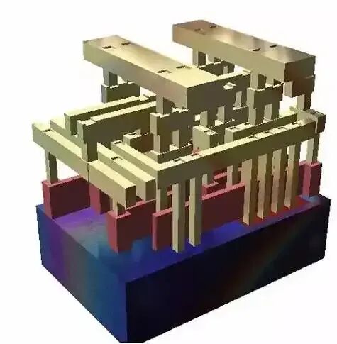
On top of the substrate are the main parts of numerous transistors. Above the substrate are many core components, such as the source, drain, and channel of the transistors.
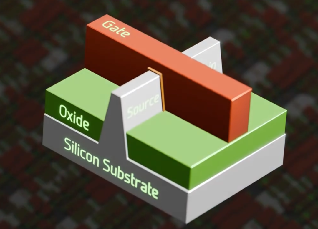
FinFET Transistor
The gate of the transistor mainly uses a “polysilicon layer”. This is because polysilicon material has better conductivity and stability, making it suitable for controlling the switching state of the transistor. The connecting metals for the source, drain, and gate of the transistor are usually tungsten.
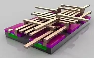
Moving further up, we need to construct numerous pathways (circuits) to connect these transistors, forming complex functional circuits.
For this connection circuit, metals are of course more suitable. Therefore, metals such as copper are mainly used. We can call this layer the metal interconnect layer.
Since everything is metal, it is easy to short-circuit. Therefore, some insulating layers (films) are also needed to isolate the circuits.
At the very top of the chip, a passivation layer is generally added. The passivation layer mainly serves a protective role, preventing contamination, oxidation, and mechanical damage from external factors (such as moisture, impurities, etc.).
So, how are all these layers built up?
The answer is thin film deposition.
This layered structure is actually formed by layer upon layer of thin films (with thicknesses ranging from sub-microns to nanometers). Some are thin metal (conductive) films, and some are dielectric (insulating) films. The process of creating these films is called deposition.
Deposition includes chemical vapor deposition (CVD), physical vapor deposition (PVD), and atomic layer deposition (ALD).
Chemical vapor deposition (CVD) is a process that generates solid materials through chemical reactions, depositing them onto the wafer to form thin films. It is commonly used to deposit insulating thin films (layers) such as silicon dioxide and silicon nitride.
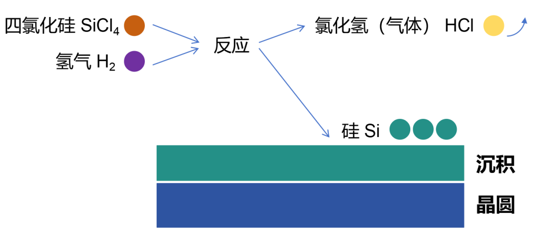
Example of Chemical Vapor Deposition
Chemical vapor deposition (CVD) has many types. Plasma-enhanced chemical vapor deposition (PECVD, which was also mentioned during oxidation) is an advanced chemical vapor deposition method that uses plasma to generate reactive gases.
This method lowers the reaction temperature, making it very suitable for temperature-sensitive structures. Using plasma can also reduce the number of deposition cycles, often resulting in higher quality thin films.
Physical vapor deposition (PVD) is a physical process.
In a vacuum environment, argon ions are accelerated to bombard the target material, causing atoms from the target material to be sputtered out and deposited on the wafer surface in a snow-like manner, forming thin films. This is physical vapor deposition.
It is commonly used to deposit metal thin films (layers) to achieve electrical connections.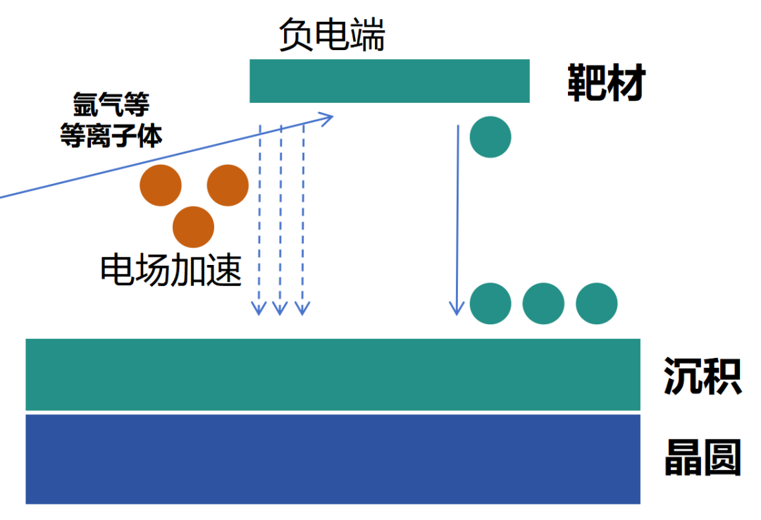 Sputtering deposition example
The process of forming metal layers (such as copper and aluminum) through thin film deposition techniques (such as PVD sputtering and electroplating) is also referred to as metallization, or metal interconnect.
Metal interconnect includes aluminum interconnect and copper interconnect. Copper has lower resistance and higher reliability (more resistant to electromigration), making it the mainstream choice today.
Atomic layer deposition (ALD) is a method that can deposit materials in the form of single atomic layers on the substrate surface, somewhat similar to ordinary chemical deposition.
Atomic layer deposition is an alternating deposition process. It first performs a chemical deposition, then uses inert gas to flush away the remaining gas, and then introduces a second gas to react chemically with the first gas adsorbed on the substrate surface. This process is repeated, with each reaction depositing only one layer of atoms.
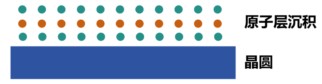
The advantage of this method is its precision. It allows for precise control of film thickness by controlling the number of deposition cycles.
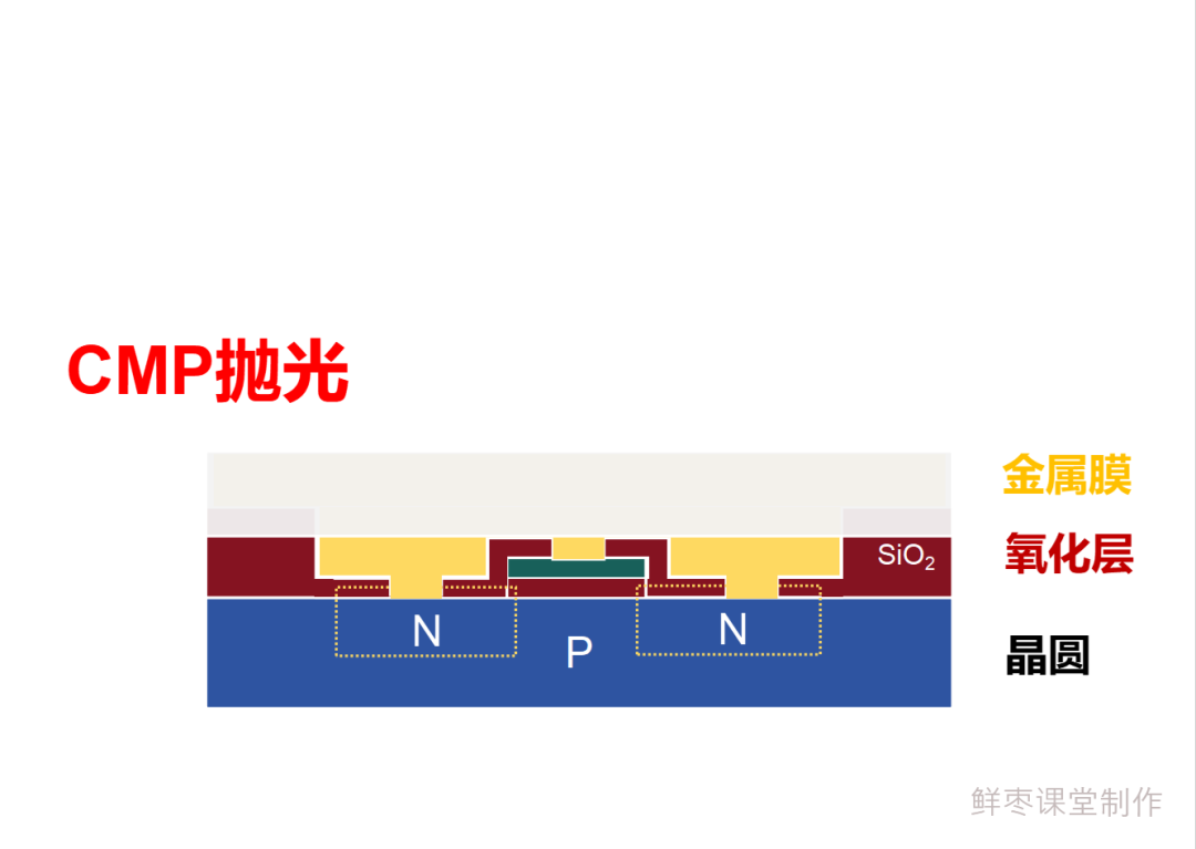
█ Cleaning and Polishing
During the processes of photolithography, etching, deposition, etc., repeated cleaning and polishing are required.
Cleaning uses high-purity chemical solutions to remove residual impurities and contaminants from the surface, ensuring the purity of subsequent processes.
Polishing eliminates surface undulations and defects on the wafer, improving the precision of photolithography and the reliability of metal interconnects, thus enabling higher density and smaller size integrated circuit designs and manufacturing.
In the previous introduction to wafer preparation, we mentioned CMP (Chemical Mechanical Polishing), which uses a combination of chemical etching and mechanical grinding to polish the wafer surface, achieving surface flattening.
If there is no CMP process, this building would be a “crooked building”. Subsequent processes cannot proceed, and the chips produced cannot guarantee quality.
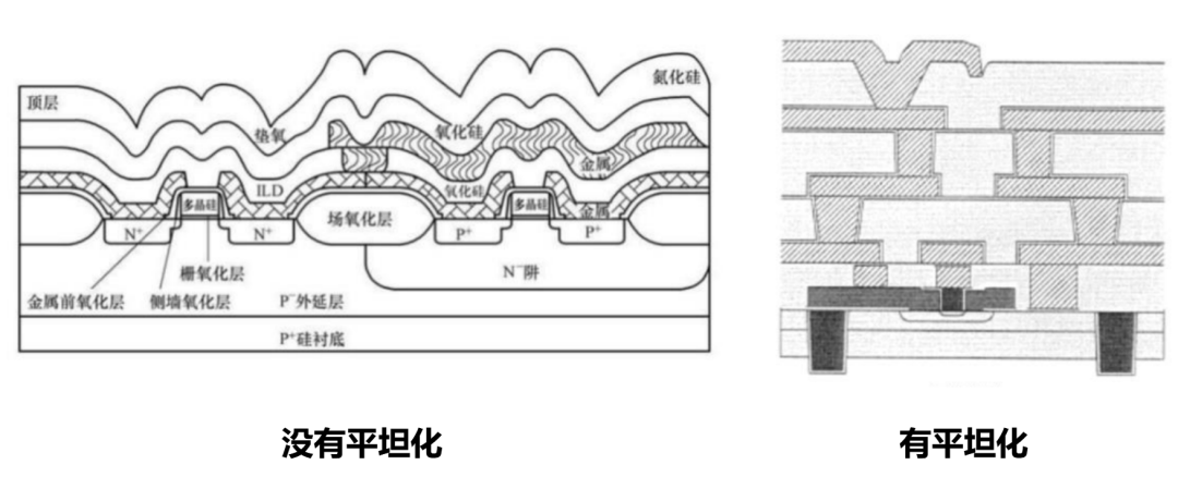
Image source: Internet
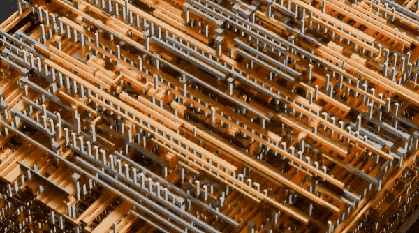
█ Repeated Cycles
As mentioned earlier, chips consist of dozens or even hundreds of layers.
In fact, the construction of each layer is a repeated cycle of photolithography, etching, deposition, cleaning, and CMP.
As shown in the GIF below:

Slow-motion breakdown:

Did everyone understand?
After N cycles of repetition, the chip building has finally “topped out”! Let’s celebrate!
But don’t celebrate too early! After “topping out”, there are still many “follow-up” processes!
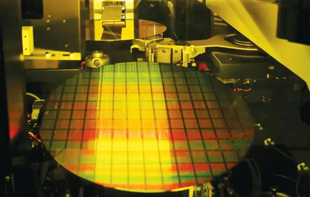
█ Probe Testing
After the previous processes, square small grids have formed on the wafer, which are the dies.
The term “Die” may surprise you at first, as it means “death” in English.
However, it has nothing to do with “death”. The term “Die” originates from the German word “Drahtzug” (wire drawing process) or is related to the cutting action “Diced”. There are also claims that early semiconductor engineers used “Die” to describe the independent units cut from the wafer, similar to coin molds.
After topping out, the first thing to do is testing.
Testing is to verify whether the quality of the semiconductor chip meets the standards. Those dies that fail the tests will not enter the packaging step, helping to save costs and time.
Electrical Die Sorting (EDS) is a testing method for wafers, usually divided into five steps, as follows:
First step: Electrical Parameter Monitoring (EPM).
EPM tests each device on the chip (including transistors, capacitors, and diodes) to ensure that their electrical parameters meet standards. The electrical characteristic data provided by EPM will be used to improve process efficiency and product performance (not for detecting defective products).
Second step: Wafer Aging Test.
The wafer is placed under certain temperature and voltage conditions for testing, which can identify products that may have early defects.
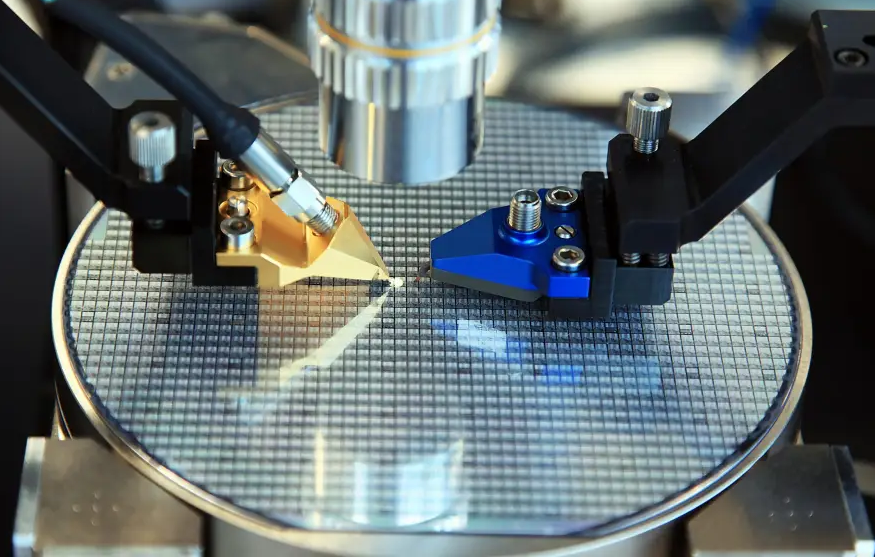
Third step: Probe Testing (Chip Probing).
At this point, the chip has not yet been cut and packaged, and its pins (or pads) are directly exposed.
Therefore, probe testing involves using precision probe stations and probe cards to connect the chip pins with automated test equipment (ATE).
ATE applies predetermined test signals to check whether the chip meets preset performance standards, such as operating voltage, current consumption, signal timing, and the correct execution of specific functions. Probe testing can also conduct electrical tests (detecting short circuits, open circuits, leakage, etc.), as well as temperature, speed, and motion tests.
Fourth step: Repair.
Yes, some defective chips can be repaired by simply replacing the problematic components.
Fifth step: Marking.
Dies that fail the tests need to be marked. In the past, we needed to use special ink to mark defective chips, ensuring they could be visually identified. Nowadays, the system automatically sorts them based on test data values.
After testing, the front-end processes of chip manufacturing are all completed! Those who have managed to read this far are true fans!
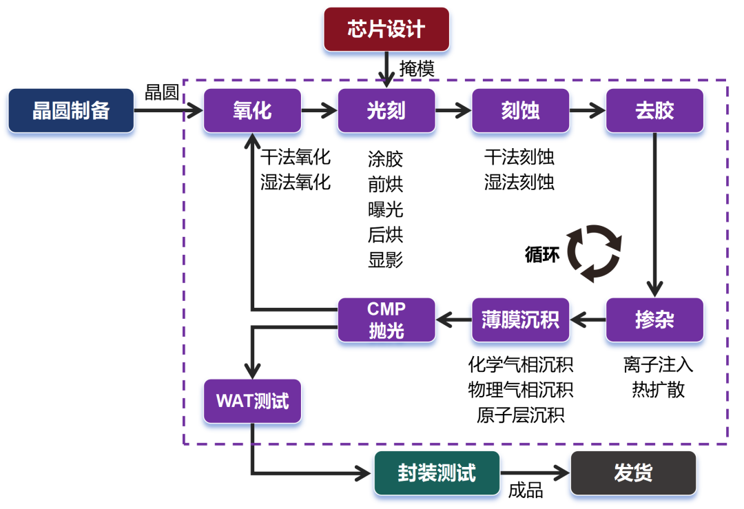
To summarize the entire process, as shown in the figure below:
References:
1. “How Chips Are Made?”, New Stone Age Park, Bilibili;
2. “Super Long Article Analyzing the Full Process of Chip Manufacturing”, Hu Shuo Man Man Tan, Bilibili;
3. “Making Chips from Sand”, Tan San Quan, Bilibili;
4. “Detailed Explanation of Chip Manufacturing Process”, Semika;
5. “Detailed Explanation of Chip Manufacturing Process”, Semiconductor Industry Observation;
6. “Detailed Explanation of Steps, Technologies, and Processes in Semiconductor Manufacturing”, Love in Qixi, Zhihu;
7. “Understanding the Entire Process of Chip Production in One Article”, Chip Semiconductor;
8. “10 Key Steps in Chip Manufacturing”, Zhongzhi Think Tank;
9. “Eight Steps in Semiconductor Product Manufacturing”, Lam Research;
10. “Steps, Technologies, and Process Diagrams in Semiconductor Manufacturing”, Beigang Nanxiang, Automotive Semiconductor Hardware, Zhihu;
11. “Understanding the Chip Production Process in One Article”, Eleanor Wool Sweater;
12. “The Birth of a Chip”, Tech Punk Roy;
13. “Full Process of Chip Manufacturing”, Zhou Jia, Chip Assistant;
14. “Semiconductor Manufacturing Technology”, Quark, Seda, Han Zhengsheng, Electronics Industry Press;
15. “Illustrated Introduction: Semiconductor Manufacturing”, Sato Junichi, Wang Yiwen, Wang Shunya, Machinery Industry Press;
16. Wikipedia, YouTube, various manufacturers’ official websites.

Recommended Reading
▊ “Detailed Explanation of Semiconductor Miniaturization Graphics and Next-Generation Photolithography Technology”“
[Japan] Okazaki Shinji, Chief Editor Zhu Guangyao, Mu Chunhang, Translated
-
“A panoramic presentation from photolithography machines to next-generation photolithography technology,” decoding every key technological innovation that drives the development of the industry.
-
29 Japanese photolithography technology experts collaborated on this work.
-
Eight domestic industry experts jointly recommend it to help China’s semiconductor industry break through difficulties.
-
From photolithography machines to next-generation photolithography technology, from photoresist materials to multiple patterning technologies, a comprehensive analysis of how each technological innovation drives the semiconductor industry towards new heights of nanometer-level precision processing.
This article is sourced from the public account “Fresh Date Classroom”
Editor: Zhang Shuqian
Reviewed by: Cao Xinyu