Shenzhen Pinghu Laboratory, in collaboration withShenzhen Pengjin High-Tech Co., Ltd., has made asignificantbreakthrough in the field ofdomesticwide bandgap semiconductor power devices! Successfully overcomingthe core technical challenges of the 1200V trench gate SiC MOSFET chip, a8-inch process platform has been established,achievinghigh-performance1200Vtrench gateSiCMOSFET chip tape-out success.Itscore invention patent(Patent Publication No.:CN118610269A) has been authorized.This marks a new level in our country’sresearch and manufacturing capabilities forkey devices of third-generation semiconductors with independent intellectual property rights, which will provide strong and lasting “Chinese chip” power for applications innew energy vehicles, photovoltaic energy storage, industrial power supplies, and more.
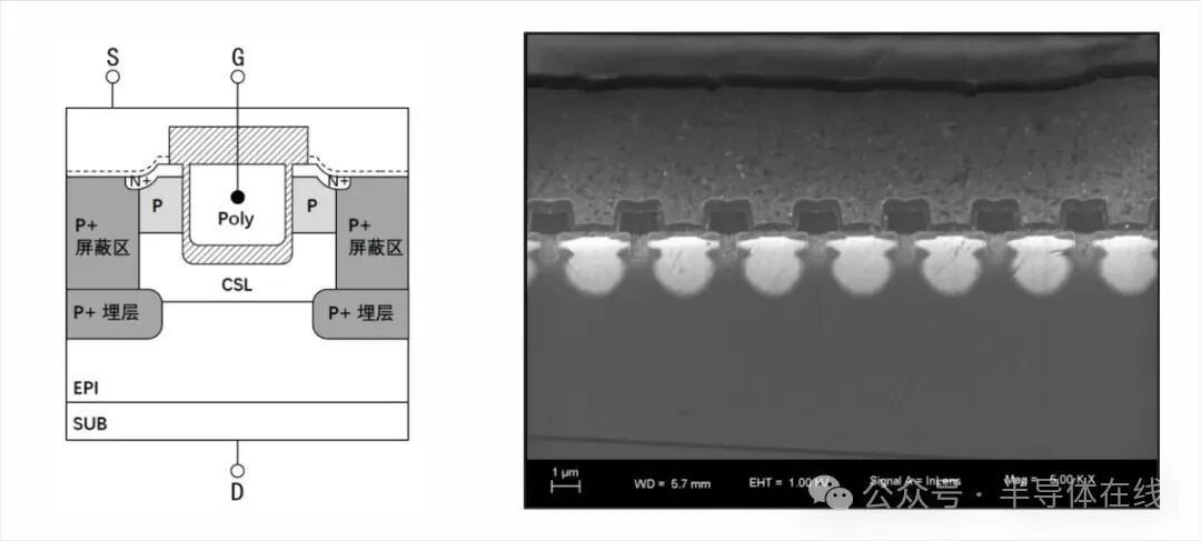
8-inch high-performance trench gateSiC MOSFET structure (patent) schematic diagram and chip cross-section

1、Outstanding performance, reliable design:
-
Static performance indicators achieve industry-leading low specific on-resistance (<2.1mΩ·cm²), surpassing the technical level of major international high-reliability manufacturers (such as Bosch G2); dynamic characteristic parameters (including input capacitance Ciss, gate charge Qg, reverse recovery charge Qrr, etc.) benchmarked against top international industrial technology standards (such as Infineon G2); overall performance reaches domestic leading and international advanced levels.
-
Zero failures achieved through 1000 hours of high-temperature reverse bias (HTRB), high-temperature positive/negative gate bias (HTGB+/-), and high-voltage high-temperature high-humidity reverse bias (HV-H3TRB) reliability assessments.
2、Sufficient robustness, wide applications:
-
While achieving high current-carrying capacity, this chip has a reverse breakdown voltage greater than1500V, with a threshold voltage stable at3.3V, demonstrating commercially viable yield on8-inch wafers, providing a solid technical foundation and enormous development potential for various application scenarios of key users.
3、Process breakthroughs, platform independence:
-
Successfully overcoming multiple SiC trench process challenges on8-inch wafers, including MeV-level high-energy ion implantation, crystal orientation etching, gate oxide thickness distribution modulation, low-defect high-temperature annealing, low resistive ohmic contact, and high-reliability passivation, achieving production-level process control.
-
Successfully established a domestically leading, internationally advanced level of fully controllable8-inch trench gateSiCMOSFET process platform, with a 1200V 40mΩ grade trench gate SiC MOSFET wafer CP yield exceeding 90%, with a single wafer reaching up to 96%. Key process controls (including trench morphology control, interface state optimization, doping uniformity, etc.) have been identified, laying a solid theoretical and technical foundation for continuous improvement of device electrical performance and mass production yield.
4、Accurate simulation, efficient design:
-
Based on the deep technical strength in SiC device physical modeling and simulation, the simulation and manufacturing alignment work of this process platform has been basically completed, from core cell structure to terminal protection structure, the full set of dynamic and static simulation and measured data correlation exceeds95%. This lays a solid foundation for subsequent rapid design optimization based on this platform.
The successful tape-out of the 8-inch 1200V trench gate SiC MOSFET chip, along with the high-quality output of the corresponding process platform and the high correlation between simulation results and measured data, represents a significant breakthrough in the core technology of third-generation semiconductors. This achievement highlights our country’s independent innovation capability and industrial strength in key links of the wide bandgap semiconductor industry chain, injecting strong momentum into the development of strategic emerging industries such as new energy and high-end manufacturing!
The National Third Generation Semiconductor Technology Innovation Center (Shenzhen), where Shenzhen Pinghu Laboratory and Shenzhen Pengjin High-Tech Co., Ltd. are located, is the world’s first open and shared research and pilot platform for 8-inch SiC and GaN, accelerating the construction process of third-generation semiconductor R&D and industrialization in our country.
Source: Shenzhen Pinghu Laboratory