As Moore’s Law approaches its physical limits, advanced packaging has become the core path for the semiconductor industry to break through performance bottlenecks. Emerging applications such as 5G, artificial intelligence (AI), high-performance computing (HPC), autonomous driving, and the Internet of Things (IoT) continuously elevate the demands for chip speed, bandwidth, power consumption, and system integration. To achieve high-density interconnection and high-performance integration, advanced packaging technologies such as Flip Chip, Fan-Out, 2.5D/3D IC, Hybrid Bonding, Chiplet, and heterogeneous integration have emerged. Major global foundries and OSAT companies are accelerating their layouts, promoting packaging innovations from wafer-level to panel-level, further unleashing computing power potential and system synergy. This report will systematically outline the definition, technical scope, key processes, material innovations, and future development trends of advanced packaging, providing deep insights and strategic references for industry participants.
01Industry Background and Development Overview
Definition and Scope of Advanced Packaging
Advanced packaging refers to a technical system that efficiently packages semiconductor chips using diverse processes and structural designs within a shell or system characterized by high performance, high density, low power consumption, and low cost. Its core lies in maximizing the integration of chip functions and optimizing interconnections to meet the trends of high-speed computing, intelligence, and miniaturization.
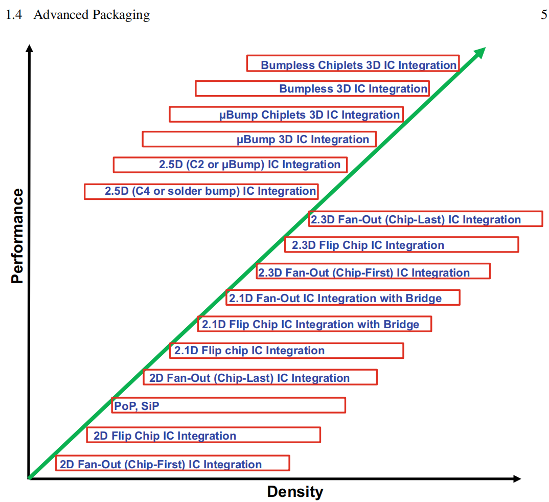
Overview of 16 Mainstream Advanced Packaging Types
The main advanced packaging methods currently adopted in the industry include: Flip Chip, Wafer/Panel-Level Chip Size Packaging (W/PLCSP), Fan-Out Wafer/Panel-Level Packaging (FOW/PLP), Package-on-Package (PoP), Through-Silicon Via (TSV), 2.1D, 2.3D, 2.5D, and 3D IC integration, High Bandwidth Memory (HBM), Multi-Chip Module (MCM), System-in-Package (SiP), heterogeneous integration, Chiplet modular packaging, and bridging technology. These packaging types each have their unique characteristics, supporting various performance and size requirements across application scenarios.
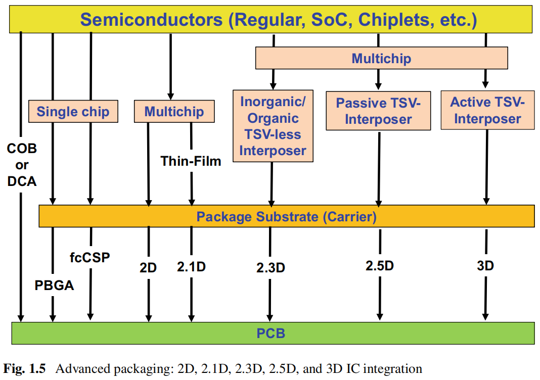
Driving Relationship Between Semiconductors and Packaging (AI, 5G, HPC, etc.)
AI (artificial intelligence) and 5G (fifth-generation broadband mobile communication technology) are the two core driving forces in the current semiconductor industry. AI has driven an exponential increase in computing power demand, while 5G has accelerated the popularity of high-speed transmission and low-latency applications. The rise of high-performance computing (HPC) and edge computing continuously challenges the speed, density, and thermal management capabilities of packaging. These trends lead to larger chip sizes, smaller pad pitches, and increased power consumption, necessitating continuous breakthroughs in packaging technology to achieve more efficient system integration.
Market Drivers and Application Scenarios
The development of advanced packaging is closely related to five core applications:
Mobile Devices:Including smartphones, tablets, and wearable devices, which impose stringent requirements for miniaturization and high performance in packaging.
Autonomous Driving:The demand for high bandwidth and low power packaging for sensors, onboard computing, and AI chips is continuously increasing.
Internet of Things (IoT):Smart homes and industrial IoT require high-reliability and low-cost packaging solutions.
Cloud Computing and Big Data:Data centers and high-performance servers rely on high-density packaging to support massive computing power and bandwidth.
Edge Computing:Real-time response scenarios require low-latency and high-efficiency packaging technologies.
The Necessity and Trends of Packaging Technology Transformation
With the push from AI, 5G, and HPC, advanced packaging has become a key path to enhance semiconductor performance. In the future, heterogeneous integration, Chiplet architecture, and 3D stacking will become major directions to support higher computing density and lower power consumption. Packaging technology will continue to evolve towards finer interconnection structures, lower loss materials, and higher reliability manufacturing processes.
02Evolution of System-in-Package
Principle of SiP (System-in-Package) Technology
System-in-Package (SiP) is a technology solution that integrates multiple functional chips, passive components, and other devices within the same package. Through organic substrates, multilayer interconnections, and high-density packaging structures, SiP can achieve more flexible system function combinations and higher integration levels. Its essence is to modularly package system-level functional modules to achieve smaller volume, lower power consumption, and higher performance goals.
Comparison of SoC and SiP
System-on-Chip (SoC) achieves system functionality by integrating multiple functional modules on the same silicon chip, but it has higher design and manufacturing costs and lower upgrade flexibility. In contrast, SiP adopts a packaging integration approach, interconnecting different chips through organic substrates, achieving system-level integration similar to SoC in functionality while offering higher design flexibility, shorter R&D cycles, and lower overall costs. Therefore, SiP is more advantageous in application scenarios requiring rapid iteration and multi-chip collaboration.
Typical Processes: SMT, Flip Chip
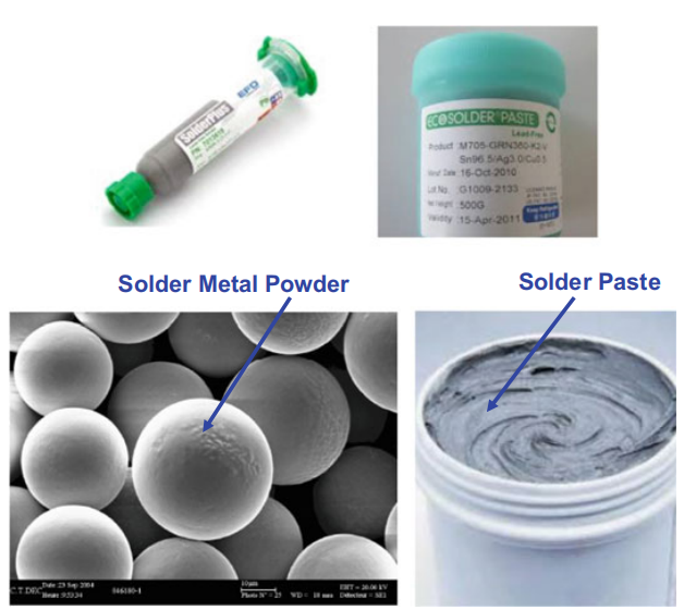
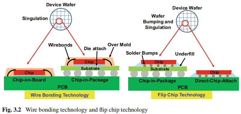
The assembly process of SiP typically employs Surface Mount Technology (SMT) and Flip Chip packaging. The SMT process includes steps such as solder paste printing, component placement, reflow soldering, AOI inspection, and rework, to achieve efficient interconnection between devices and printed circuit boards (PCBs). The Flip Chip process involves forming bumps (C4 or C2 Bump) on the wafer and then directly mounting the chip face down onto the substrate through thermal compression or reflow soldering, achieving high I/O density and excellent electrical performance. To enhance packaging reliability, Flip Chip assembly is usually combined with underfill materials to mitigate thermal stress.
Practical Applications and Typical Case Analysis
SiP technology has been widely applied in mobile devices, smart wearables, IoT modules, RF front-end modules, and high-performance computing fields. It can integrate sensors, memory, processors, and power management chips to achieve high functional density and extreme miniaturization. Typical cases include the SiP packaging solution for multifunctional RF modules in advanced smartphones and the high-density packaging in wearable devices utilizing a combination of Flip Chip and SMT to optimize volume and enhance performance.
03Wafer and Panel-Level Packaging
Fan-In Wafer/Panel-Level Chip-Scale Package (WLCSP/PLCSP)
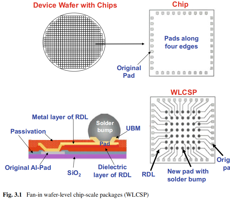
Fan-In Wafer/Panel-Level Chip Size Packaging (WLCSP/PLCSP) is an important form of advanced packaging characterized by using a redistribution layer (RDL) to route the I/O ports of the chip while keeping the packaging area close to the chip size. WLCSP achieves high integration and miniaturization through packaging processes at the wafer level, while PLCSP processes on larger panels enhance production efficiency and reduce costs. Typical processes include wafer dicing, molding, reflow soldering, thermal cycling testing, and failure analysis. Fan-In packaging is particularly suitable for mobile devices and consumer electronics due to its significant advantages in packaging height and size.
Fan-Out Wafer/Panel-Level Packaging (FOWLP/FOPLP)
Fan-Out packaging breaks through the limitations of chip size by redistributing I/O ports around the chip, achieving higher I/O density and better electrical performance. Its processes are mainly divided into Chip-First and Chip-Last categories. The Chip-First method arranges the chip on the wafer before redistributing, while the Chip-Last method forms the redistribution structure first and then places the chip, suitable for high reliability and high-density packaging. FOWLP is suitable for mobile application processors, RF modules, and high bandwidth memory, while FOPLP can significantly reduce unit costs by leveraging the process advantages of large panels.
Reliability and Testing Methods of Wafer and Panel-Level Packaging
In wafer and panel-level packaging, thermal cycling testing, drop testing, and finite element simulation analysis are common reliability verification methods. By analyzing the stress on the packaging structure and studying failure modes, the strength of solder joints and material compatibility can be optimized to enhance the long-term stability of the overall product.
042D to Multidimensional Packaging Integration
2D, 2.1D, and 2.3D IC Integration
2D packaging mainly employs traditional wire bonding and Flip Chip technologies, suitable for applications with relatively low I/O count and interconnection density requirements. As chip functions continue to enhance, 2.1D and 2.3D integration have gradually emerged. 2.1D packaging achieves interconnection between chips through organic interposers, while 2.3D packaging further realizes high-density integration of multiple chips on organic substrates or RDL (Redistribution Layer), balancing performance and flexibility. These solutions support heterogeneous integration of multiple chips, enhancing signal transmission speed and reducing packaging height.
2.5D IC Integration
2.5D packaging utilizes Through-Silicon Via (TSV) and passive silicon interposers to achieve lateral multi-chip high-density interconnection. Typical representative processes include TSMC’s CoWoS technology and applications by Xilinx and AMD in high-performance computing chips. 2.5D integration significantly improves bandwidth density and thermal management capabilities, widely used in GPU, AI accelerators, and high bandwidth memory (HBM) modules.
3D IC Integration and 3D Packaging
3D packaging achieves high bandwidth and low latency interconnections by vertically stacking multiple chips using TSV or hybrid bonding. Common forms include HBM stacked memory, Package-on-Package (PoP) structures, and Chip-on-Chip integration. Compared to 2.5D, 3D packaging has greater advantages in area utilization and signal transmission paths but faces higher challenges in thermal management and manufacturing yield.
Key Materials and RDL Technology
RDL, as the core interconnection structure between chips and packaging, encompasses organic, inorganic, and hybrid material solutions. Advanced RDL must meet high-frequency low-loss (Low Dk, Df) and thermal stability requirements to cope with the stringent performance demands of 5G, AI, and HPC application scenarios.
05Key Frontier Technologies
Hybrid Bonding
Hybrid bonding is one of the frontier technologies for achieving high-density, low-latency interconnections. It directly bonds metal-to-metal (Cu-Cu) or dielectric-to-dielectric (SiO₂-SiO₂), achieving smaller interconnection pitches and higher signal transmission efficiency. Thermal compression bonding (TCB) is its core process, including high-temperature Cu-Cu bonding, room-temperature Cu-Cu bonding, and SiO₂-SiO₂ bonding schemes. In recent years, low-temperature hybrid bonding technology has rapidly developed, enhancing packaging reliability and reducing thermal stress. Companies such as Sony, TSMC, Intel, and IMEC have widely applied hybrid bonding technology in CMOS image sensors, 3D ICs, and HBM packaging to meet the demands of 5G and high bandwidth memory.
Chiplet and Heterogeneous Integration
The Chiplet architecture is becoming the core design concept for the next generation of high-performance computing. Compared to traditional single SoCs, Chiplets modularly integrate multiple functional chips (computing units, I/O modules, memory controllers, etc.) within the same package, shortening R&D cycles and reducing manufacturing costs.
Heterogeneous integration technology combines various packaging forms, including 2D Chiplets on organic substrates, high-bandwidth interconnections on 2.5D silicon interposers (Passive TSV Interposer), and vertical integration of 3D TSV stacking or hybrid bonding. AMD’s multi-chip architecture (Epyc and Ryzen processors), Intel’s EMIB technology, and TSMC’s InFO series packaging are typical practices of Chiplet and heterogeneous integration.
Advantages and Challenges
Chiplet heterogeneous integration can achieve flexible combinations of functions, improving yield and design flexibility, but challenges remain in high-speed signal transmission, thermal management, power consumption, and standardized interfaces. To address these issues, the industry is promoting the joint development of advanced packaging platforms (such as CoWoS, Foveros) and unified interconnection standards to meet the system-level demands of AI, high-performance computing, 5G, and autonomous driving chips.
06Material and Manufacturing Innovations
Low-Loss Dielectric Materials (Low Dk, Df)
With the rapid development of 5G, AI, and high-performance computing (HPC), packaging materials have higher requirements for high-speed signal transmission. Low dielectric constant (Dk) and low dielectric loss (Df) dielectric materials can effectively reduce signal delay and power consumption, enhancing high-speed interconnection performance. Currently, major industry suppliers (such as DuPont, JSR, Hitachi, Arakawa, etc.) have developed various organic and inorganic dielectric materials that meet high-frequency, low-loss requirements. These materials not only possess excellent electrical properties but also have low coefficients of thermal expansion (CTE) to reduce deformation and failure of packaging structures caused by thermal stress.
Assembly and Testing of Advanced Packaging
The manufacturing of advanced packaging involves various key processes, including SMT (Surface Mount Technology), Flip Chip packaging, Chip-on-Chip (CoC), Wafer-on-Wafer (WoW), and other multi-level integration technologies. Key steps in the assembly process include:
Wafer Bumping and RDL Manufacturing:Achieving high-density I/O interconnections through C4 (Controlled Collapse Chip Connection) or C2 Bump technology.
Flip Chip Assembly:Installing the chip face down through reflow soldering or thermal compression (TCB), combined with underfill to enhance packaging reliability.
Reflow Soldering and AOI Inspection:Precision mounting and automatic optical inspection of SMD (Surface Mounted Devices) to ensure quality.
Packaging Testing and Failure Analysis:Including thermal cycling testing, drop testing, X-Ray inspection, and finite element simulation analysis to verify the long-term reliability of the packaging.
07Trends and Strategic Insights
Industry Trends and Market Drivers
Advanced packaging is gradually replacing traditional packaging, becoming the core driving force for enhancing semiconductor performance and expanding functionality. As Moore’s Law approaches physical limits, packaging has evolved from “device protection” to a critical link in “system integration.” In the future, 2.5D and 3D ICs, Chiplet architectures, and heterogeneous integration technologies will continue to expand market share, driving the demand for high bandwidth, low power consumption, and high integration. Major global foundries and OSAT manufacturers are accelerating investments to enhance packaging capacity and technical capabilities, ensuring competitive advantages in high-performance computing, 5G, and AI applications.
Strategic Comparison of SoC and Chiplet
System-on-Chip (SoC) integrates multiple functional modules through a single chip, achieving high performance and miniaturization, but its design and manufacturing costs are high and lack flexibility. The Chiplet architecture, on the other hand, breaks down functions into multiple small chips, achieving modular splicing through advanced packaging, enhancing design flexibility, improving wafer yield, and shortening R&D cycles. With the maturity of 2.5D and 3D packaging, the Chiplet architecture has become the preferred solution in data centers, AI accelerators, and high-end GPUs.
Future Development Directions and Technical Recommendations
Heterogeneous Integration and Systematic Packaging:Integrating logic chips, memory, RF, and power management modules to achieve multi-functional collaboration.
Material and Process Innovations:Developing lower Dk/Df dielectric materials and high-reliability interconnection structures to meet high-speed signal and low power consumption demands.
Advanced Interconnection Technologies:Hybrid bonding, TSV, and RDL optimization will continue to enhance interconnection density and bandwidth.
Smart Manufacturing and Automation:Introducing AI-driven inspection and process control to improve packaging yield and production efficiency.
Investment and Strategic Opportunities
With the rapid rise of 5G, AIoT, smart vehicles, and cloud computing, the market space for advanced packaging will significantly expand. In the next five years, the market growth rate of Chiplet and 3D IC will far exceed that of the overall semiconductor industry. Leading companies need to build differentiated competitive barriers in advanced packaging through ecosystem collaboration, platform standardization, and investment in technology R&D.
(Source: Semiconductor Industry Report. This article is produced by the Qingdao West Coast International Investment Promotion Center, reprinted for sharing and learning purposes only, not for commercial use. If there is any infringement, please contact for deletion.)
 NEXT
NEXT

Qingdao West Coast New Area International Investment Promotion Center
Mainly responsible for the new display, integrated circuits, software information technology, and technology service industrial chains in the West Coast New Area, as well as investment promotion work in the direction of the new generation of information technology and future industries in Qingdao’s “10+1” innovative industrial system.
Investment Hotline:
0086-532-86989002
Recommended Reading
Over 500 million in taxes paid in 4 years! Zhuanzhuan Group settles in Qingdao West Coast, nurturing a benchmark for circular economy in a fertile business environment

Qingdao West Coast New Area: Striving for New Heights, Strengthening the Manufacturing Industry

Policy Update | Key Project Management Measures for Green, Low-Carbon, and High-Quality Development in Shandong Province