Comprehensive Guide to Advanced Semiconductor Packaging (Part 2)
Comprehensive Guide to Advanced Semiconductor Packaging (Part 2)

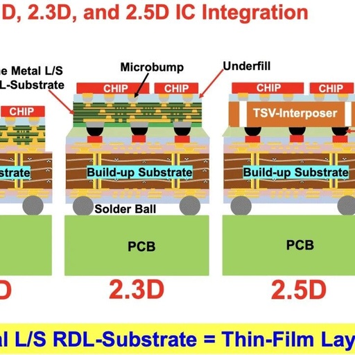
[Image]【Table of Contents】1. Electronic Packaging Overview 2. Early Packaging Types 3. 2D: Flip Chip Packaging 4. 2D: Wafer-Level Packaging 5. The Rise of Advanced Packaging 6. 2.1D/2.3D: Ultra-Thin Organic Interposers 7. 2.5D: Silicon Interposers, Microbumps, Silicon Through-Silicon Vias, and Silicon Bridges 8. 3D-IC Packaging 9. Hybrid Bonding 2.1D/2.3D: Ultra-Thin Organic Interposers (Inte…
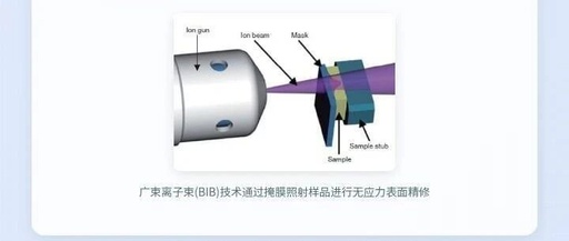
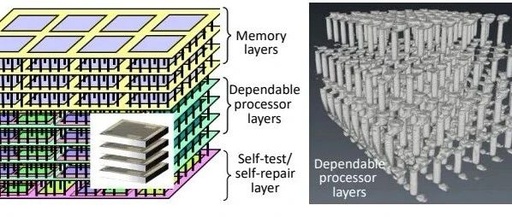
Democratizing 3D Integration: A Low-Cost Prototyping Solution Based on Chip-Level Thinning, Through-Silicon Vias (TSV), and Meta Bonding

Democratizing 3D Integration: A Low-Cost Prototyping Solution Based on Chip-Level Thinning, Through-Silicon Vias (TSV), and Meta Bonding

Original link: https://xplorestaging.ieee.org/document/11007580【Abstract】 Three-dimensional integrated circuit (3D-IC) technology, with its vertical interconnections through silicon vias (TSV), has become central to advanced semiconductor devices. However, the initial development costs are prohibitively high, primarily due to the substantial investment required for wafer-level TSV processes. This study proposes…

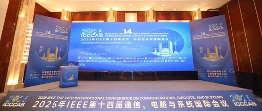
ICCCAS 2025: Silicon Core Technology Shares Insights on Advanced Packaging Technology Exploration and Layout

ICCCAS 2025: Silicon Core Technology Shares Insights on Advanced Packaging Technology Exploration and Layout

ICCCAS 2025 The 14th IEEE International Conference on Communications, Circuits and Systems (ICCCAS 2025) will be grandly held in Wuhan from May 23 to 25, 2025, co-hosted by IEEE, Wuhan University of Technology, and University of Electronic Science and Technology of China. A total of 170 scholars and researchers from universities and research institutions in … Read more