Click to receive a free sample coupon~


In the field of electronic manufacturing, PCBs serve as the “nervous system” of electronic products, and the quality of their design directly determines the performance and reliability of the products. However, some seemingly reasonable PCB designs may hide fatal flaws, becoming time bombs for product failure. This article will delve into the hidden issues in PCB design.
1. The Invisible Traps of Layered Structures
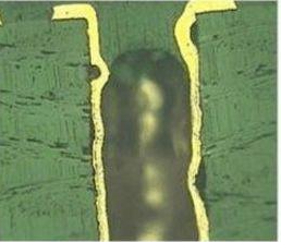
In a 6-layer communication board, a deviation of 5μm in the dielectric layer thickness can cause a characteristic impedance fluctuation of ±8Ω, leading to signal reflection and a 3ns oscillation in the rising edge. More seriously, a medical device’s mainboard experienced coupling interference between the 12V power layer and the signal layer due to a 0.1mm misalignment between layers, resulting in a 2LSB offset in ADC sampling values. These issues are like invisible traps; a slight misstep can lead to decreased product performance or even failure.
2. The Fatal Blind Spots of Thermal Design
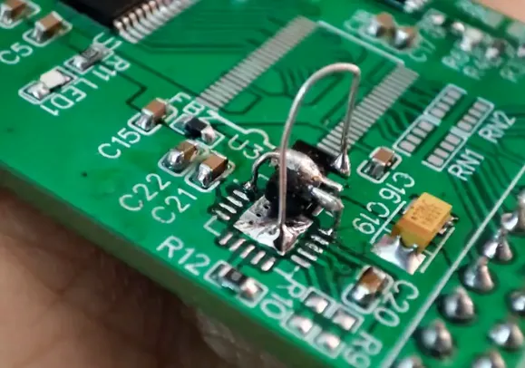
Thermal design is a crucial guarantee for PCB reliability. The FR4 substrate undergoes thermal decomposition at sustained high temperatures, with the Tg value dropping from 135°C to 110°C, and the copper foil peel strength decreasing by 40%. This thermal design flaw not only affects material performance but may also lead to component failure. An improved honeycomb heat dissipation hole design reduced hotspot temperatures by 22°C, increasing MTBF (Mean Time Between Failures) to 50,000 hours, fully demonstrating the importance of scientific thermal design.
3. The Domino Effect of Signal Integrity
Signal integrity issues are often like a domino effect in PCB design; once a problem occurs in one link, it can trigger a chain reaction. After re-layout using the 3W principle, crosstalk was reduced by 18dB, and signal quality improved by 35%. This case illustrates that signal integrity issues cannot be ignored; any minor oversight can lead to serious consequences.
Design Guidelines
1. Using 3D electromagnetic field simulation can detect 90% of signal integrity issues in advance. The professional simulation tools from Jiepei PCB can provide engineers with accurate modeling and analysis, helping them optimize designs and avoid potential signal problems.
2. Thermal simulation can control temperature differences within 15°C. Jiepei PCB’s thermal design services can develop scientifically reasonable heat dissipation plans based on specific product needs, ensuring stable operation under various working conditions.
3. Retaining 20% of routing margin can effectively cope with production tolerances. Jiepei PCB strictly controls process parameters during production to ensure the rationality and stability of routing margins, improving product manufacturability and reliability.
4. Choosing materials with stable Dk values can reduce transmission losses by 3%. Jiepei PCB has established strategic partnerships with top global board material suppliers to ensure that the materials provided have excellent electrical performance and stability, providing a solid guarantee for high-performance product operation.
Hidden issues in PCB design are like lurking time bombs, potentially triggering product failures at any moment.
Some images in this article are sourced from the internet; please contact us for removal if there is any infringement.
END
Previous/Review
REVIEW

The Hidden Killer During Soldering: How Solder Smoke Harms Our Bodies?

What Are the Obvious Signs That a Hardware Engineer Is Incompetent?
I Don’t Believe You Haven’t Flown! Why Is Hardware Design So Challenging?
You spent · reading
Click below to read the original text and register as a member to receive a free sample coupon!