10-Layer First-Level HDI PCB Manufacturing Process and Technical Points
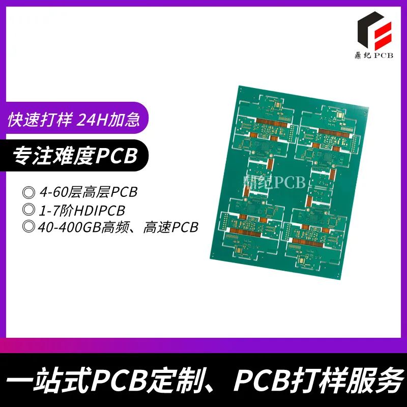
1. Definition and Features of 10-Layer First-Level HDI Board
The 10-Layer First-Level HDI (High-Density Interconnect) board is a type of multi-layer PCB that uses blind hole technology to connect the outer and inner layers, structured as 1+8+1, which means 1 outer layer, 8 inner layers, and 1 additional outer layer. Its features include:
– High-Density Wiring: Achieved through blind and micro-hole technology for high-density interconnect.
– Simplified Process: Requires only one outer layer copper foil lamination and one laser drilling.
– Cost Advantage: Compared to higher-level HDI, the manufacturing process of first-level HDI is relatively simple and cost-effective.
2. Manufacturing Process
The manufacturing process of the 10-Layer First-Level HDI board involves several key steps, detailed as follows:
1. Material Preparation
– Substrate: Typically made from FR-4 high Tg materials, which have good insulation and thermal stability.
– Copper Foil: The thickness of the outer and inner layer copper foil is generally 1 ounce.
– Prepreg: Used for interlayer bonding to ensure the stability of the multilayer structure.
2. Inner Layer Circuit Production
– Pattern Transfer: Transfer the designed circuit diagram onto the inner layer substrate using photolithography technology.
– Etching: Remove excess copper layers through chemical etching to form the desired circuit.
– Blackening and Browning: Treat the inner surface to enhance interlayer bonding strength.
3. Multilayer Lamination
– Inner Layer Lamination: Laminate the 8 inner layer boards together using prepreg.
– Outer Layer Lamination: Laminate one layer of outer copper foil on both sides of the inner layer board.
4. Hole Processing
– Blind Hole Drilling: Use laser drilling technology to create blind holes connecting the outer and inner layers.
– Electroplating Filling: Fill the blind holes with copper through electroplating to ensure conductivity.
5. Outer Layer Circuit Production
– Pattern Transfer: Transfer the outer layer circuit diagram onto the outer copper foil.
– Etching: Etch the outer copper foil to form the final outer layer circuit.
6. Surface Treatment
– Gold Plating or Tin Spraying: Perform surface treatment on the outer layer to improve solderability and corrosion resistance.
7. Testing and Inspection
– Electrical Testing: Check the continuity and insulation performance of the circuits.
– Appearance Inspection: Inspect for surface defects to ensure product quality.
3. Technical Points
1. Laser Drilling Technology
– Laser drilling is a key process for HDI boards, capable of achieving extremely small hole diameters (usually less than 0.2mm), increasing wiring density.
2. Interlayer Alignment Precision
– High precision alignment is required during multilayer lamination to ensure the reliability of interlayer electrical connections.
3. Electroplating Filling
– Electroplating filling process needs strict control to ensure the uniformity and conductivity of the copper layer inside the blind holes.
4. Material Selection
– Select appropriate substrate and copper foil thickness to balance cost and performance.
4. Application Scenarios
The 10-Layer First-Level HDI board is widely used in the following fields:
– Consumer Electronics: Such as smartphones and tablets, meeting the demand for miniaturization and high performance.
– Communication Equipment: Such as 5G base stations and routers, supporting high-speed data transmission.
– Automotive Electronics: Such as in-vehicle infotainment systems, required to operate stably in harsh environments.
5. Conclusion
The 10-Layer First-Level HDI board balances high performance and cost through simplified processes and high-density designs. Its manufacturing process involves critical steps such as multilayer lamination, laser drilling, and electroplating filling, making it suitable for high-end electronic products with requirements for wiring density and cost.