After completing the PCB design, to ensure smooth production and meet subsequent maintenance needs, the following key documents are typically required:
- 1. PCB Production Documentation
- • Gerber files
- • Drill files
- • IPC netlist (optional)
- • PCB fabrication instructions
- • Coordinate files
- • BOM (Bill of Materials)
- • Assembly drawings (optional)
- • 3D model files (optional)
- • Interactive BOM, useful for manual soldering (optional) AD implementation of interactive BOM output in Kicad format
- • PCB design source files
- • Schematic files
- • Test point files (optional)
- • Impedance control requirements table<**optional**> (stack-up table)
- • Fabrication requirements documentation (process requirements)
⚙️ 1. Main Contents of PCB Production Documentation
Gerber Files (File format: RS-274X is the most commonly used)
- • Photoplot files for each layer:
- • Top/Bottom copper foil (Top/Bottom Layer)
- • Solder mask layer (Solder Mask)
- • Silkscreen layer (Silkscreen)
- • Drill layer (Drill Drawing)
- • Inner layers (for multilayer boards)
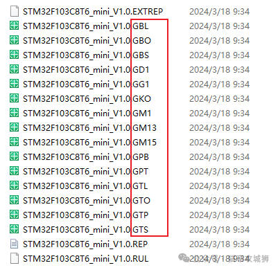
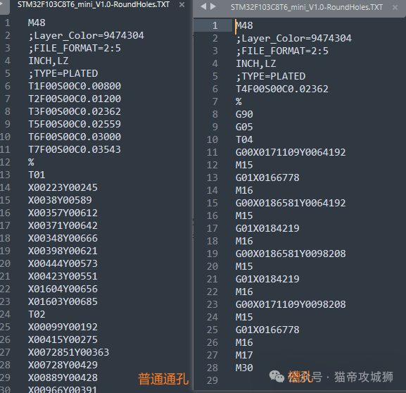
Gerber Files - • Drill Files (NC Drill Files)
- • Contains coordinates and hole diameter information for through holes and vias (.drl or .txt).
- • May be divided into blind/buried holes, slot holes, and through hole files.
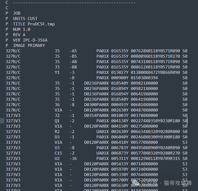
Drill Files - • IPC Netlist File (optional)
- • Provides the PCB manufacturer with a means to verify that the electrical connections are correct after PCB fabrication (.ipc or .net).
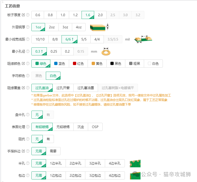
IPC Netlist - • PCB Fabrication Instructions (TXT/PDF)
- • Board thickness, materials (e.g., FR4), surface processes (gold plating, tin spraying, etc.), impedance requirements, special process instructions, etc.
- • If ordering from online stores like JLCPCB, Huachuang, or Jietong, there is no need to write separate fabrication instructions; you can select them directly when placing the order.
Online Selection of Process Information – Huachuang
🔧 2. SMT Placement Files (Assembly Documentation)
- • Coordinate Files (Pick and Place File)
- • Component designators, coordinates, rotation angles, package names (.csv or .txt).
- • Must distinguish between top and bottom layer components.
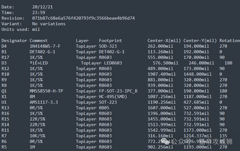
Coordinate Files - • BOM (Bill of Materials)
- • Component designators, part numbers, parameters, quantities, manufacturer part numbers, placement methods, etc. (.xls or .csv).
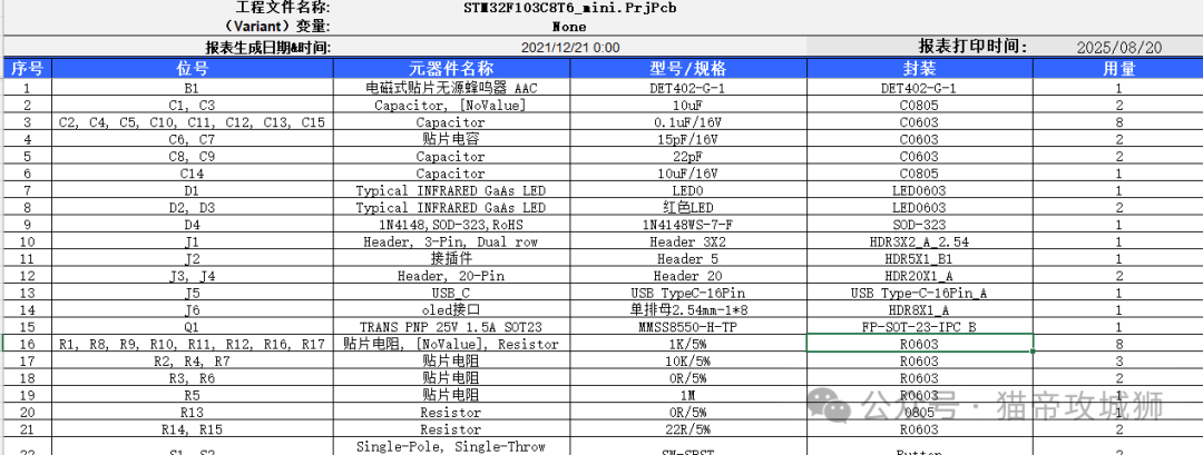
BOM - • Assembly Drawings (Assembly Drawing)
- • Generally in PDF format, indicating component locations, polarity, orientation, etc.
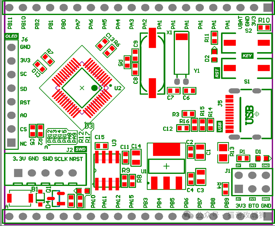
Assembly Drawing - • 3D Model Files (optional)
- STEP format (.stp), used for structural verification, thermal simulation, or rendering effects.
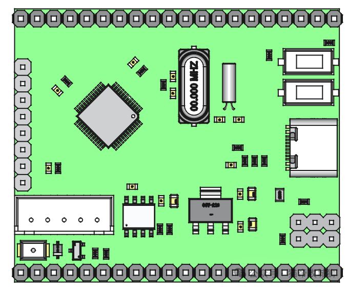
3D Model – View 🔌3. Stencil Files (Solder Paste Layer)
- • Top/Bottom stencil Gerber (Paste Mask layer), made in two separate parts, can be omitted if there are no surface mount devices on the bottom layer, used for making solder paste stencils (applicable for cases where stencils are made separately).
- • This item is generally also optional, and it is usually possible to request the PCB manufacturer to return production documentation (stencil data), using it to make the stencil; if the PCB manufacturer can directly make the stencil, it is even simpler, just need to associate it with the PCB production order to produce the stencil files.
-
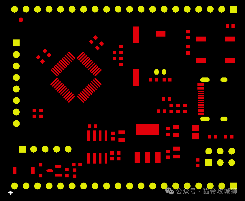
Stencil Data Preview
🚀 4. Organization of Design Files (indicating version number, modification date, change content, etc.)
- • PCB Design Source Files
- • Original project files (e.g., Altium’s .PcbDoc, Cadence’s .brd, KiCad’s .kicad_pcb).
- • Schematic Files
- • Schematics (.SchDoc, .sch) and library files (.Lib).
- • Test Point Files (optional)
- • Indicating test point locations, network names, for ICT or flying probe testing.
- • Impedance Control Requirements Table<**optional**> (stack-up table)
- • High-speed designs need to provide stack-up impedance design and requirements table (e.g., differential pair impedance, layer thickness parameters).
- • Can output a separate documentation file, or can place the stack-up table in the PCB;
- • Fabrication Requirements Documentation (process requirements)
- • Board material type (e.g., FR4, high-frequency materials), copper thickness (1oz/2oz);
- • Surface processes (gold plating, tin spraying, ENIG);
- • Character color (generally white), PCB solder mask color (default green);
- • Board thickness (0.8mm, 1mm, 1.6mm, 2mm);
- • Special requirements: impedance control, blind/buried vias, stamp holes, V-cut, etc.
————>> THE END <<————
 Please like and follow
Recommended reading for BOM organization:
A formula to solve BOM NC value organization techniques
Master Altium Designer: Easily customize your own BOM format template
No plugins needed, quickly generate interactive BOM (soldering tools) using Huachuang DFM