Power supply circuits are an important component of electronic products. The quality of power supply circuit design directly affects product performance. The main types of power supply circuits in our electronic products are linear power supplies and high-frequency switching power supplies. Theoretically, a linear power supply provides as much current as the user needs at the input; a switching power supply provides as much power as the user needs at the input.
Linear Power Supply
Linear power supply power devices operate in a linear state, such as the commonly used voltage regulator chips LM7805, LM317, SPX1117, etc. 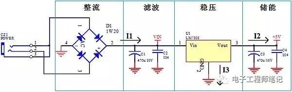 Figure 1: Linear Power Supply Schematic
As can be seen from the diagram, a linear power supply consists of components for rectification, filtering, voltage regulation, and energy storage. Generally, the linear power supply is a series voltage regulator, where the output current equals the input current, I1=I2 I3, with I3 being the reference terminal and a very small current, thus I1≈I3. The reason we discuss current is that in PCB design, the width of each line is not arbitrary; it must be determined based on the current magnitude between component nodes in the schematic (please refer to the “PCB Design Copper Thickness, Line Width, and Current Relationship Table”). Understanding the size and direction of the current is crucial for making the board appropriately.
In PCB design, the layout of components should be compact, with all connections as short as possible, arranged according to the functional relationships of the components in the schematic. In this power circuit, rectification is done first, followed by filtering, then voltage regulation, and finally energy storage capacitors, which supply power to the subsequent circuits after passing through the capacitors. 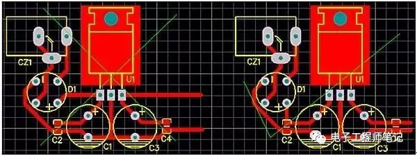 Figure 2: Linear Power Supply PCB
When designing a linear power supply PCB, attention should also be paid to the heat dissipation of the voltage regulator chip. Heat is generated based on the voltage drop across the regulator. If the input voltage is 10V and the output voltage is 5V with an output current of 500mA, the voltage drop across the regulator is 5V, resulting in a heat generation of 2.5W; if the input voltage is 15V, the voltage drop is 10V, generating 5W of heat. Therefore, we must leave enough space for heat dissipation or use appropriate heat sinks based on the heat dissipation power. Linear power supplies are generally used in situations with small voltage differences and low currents; otherwise, please switch to a switching power supply circuit.
High-Frequency Switching Power Supply
A switching power supply uses a circuit to control a switch transistor to conduct and cut off at high speed, generating a PWM waveform, which is then regulated through inductors and freewheeling diodes, utilizing electromagnetic energy conversion. Switching power supplies have high power, efficiency, and low heat generation. Common circuits include LM2575, MC34063, SP6659, etc. Theoretically, the power across the switching power supply should be equal, with voltage inversely proportional and current inversely proportional. 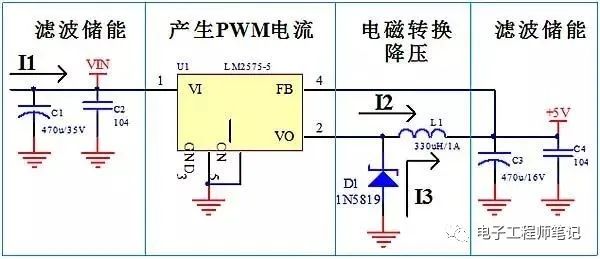 Figure 3: LM2575 Switching Power Supply Schematic
When designing the PCB for a switching power supply, attention should be paid to the feedback line entry point and to whom the freewheeling diode is providing current. As shown in Figure 3, when U1 is conducting, the current I2 enters the inductor L1. The characteristic of an inductor is that the current flowing through it cannot suddenly change or disappear; the change in current through the inductor takes time. Under the influence of the pulsed current I2 flowing through the inductor, some electrical energy is converted into magnetic energy, causing the current to gradually increase. At a certain point, the control circuit U1 turns off I2, and due to the inductor’s characteristics, the current cannot suddenly disappear; this is where the diode comes into play, taking over the current I2, hence it is called a freewheeling diode. The freewheeling current I3 flows from the negative terminal of C3, through D1 and L1, to the positive terminal of C3, akin to a pump using the inductor’s energy to elevate the voltage across capacitor C3. Additionally, the feedback line entry point for voltage detection should be after filtering; otherwise, it will increase the output voltage ripple. These two points are often overlooked by many PCB designers, who mistakenly believe that connecting to the same network at different points yields the same result; in fact, the performance impact is significant. 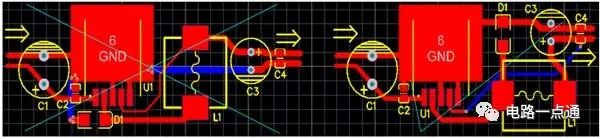 Figure 4: LM2575 Switching Power Supply PCB
We emphasize the importance of understanding the schematic because it contains much information necessary for PCB layout, such as connection points for component pins and the current magnitudes of node networks. Once the schematic is clear, PCB design becomes straightforward. The LM7805 and LM2575 circuits represent typical layouts for linear and switching power supplies, respectively. When creating PCBs, simply follow the layout and wiring of these two types of PCB diagrams, with adjustments made according to the specific product.
Ultimately, the principles and layout methods of all power supply circuits are consistent, and every electronic product relies on power and its circuits. Therefore, mastering these two circuits will provide clarity on others as well.
Copyright Statement:This article is copyrighted by the original author and does not represent the association’s views.The articles shared by the “Jiangxi Province Electronic Circuit Industry Association” are for sharing purposes only and do not represent the stance of this account. For copyright issues, please contact us for deletion.