
The wave soldering process of PCBA components is a major stage that leads to defects, with a defect rate as high as 50% throughout the PCBA assembly process. The defects that occur during wave soldering can be seen as a concentrated manifestation of problems in previous manufacturing processes, and these defects can be categorized into obvious and hidden types. Obvious defects are relatively easy to detect, but the focus is more on hidden defects. Therefore, this chapter will focus on the defects that exist in both lead-free and leaded wave soldering.
The common defects include cold solder joints, poor wetting, de-wetting, poor solder joint formation, bridging, solder spikes, poor through-hole soldering, voids, pinholes, “explosive” holes, disturbed or fractured solder joints, dark solder joints, or granular solder joints.
The appearance of a cold solder joint is characterized by a rough, grainy surface with poor luster and flowability. Essentially, if a proper thickness of the intermetallic compound (IMC) layer is not formed at the interface of the joint during the soldering process, it can be deemed a cold solder joint. Upon tearing a solder joint, it can be found that there is no residual mixture between the base metal and the solder, and the interface is flat and clear, as if glued together. In contrast, a normal solder joint will show intermingled cracks between the base metal and the solder, with solder residue on the base metal and traces of the base metal on the solder.
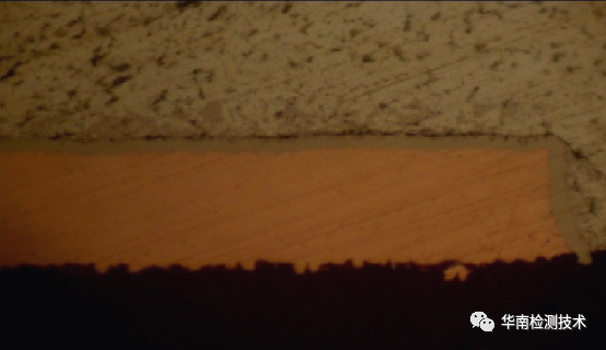
The connection interface of a cold solder joint neither undergoes wetting nor diffusion, appearing as if glued together. The solder joint surface exhibits a rough shape, poor luster, and a contact angle θ greater than 90°, as shown in the figure below. In this case, there exists an unweldable thin film between the solder and the base metal interface, obstructing the ideal metallurgical reaction from occurring. This apparent cold solder joint phenomenon can be judged from its appearance.
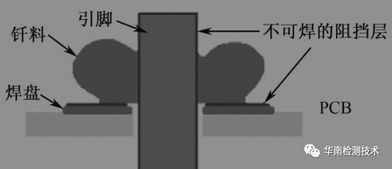
Why do metals join together and form connection strength through soldering?
Taking the commonly used Sn-37Pb alloy solder as an example, under the influence of soldering temperature, it wets the surface of the joining metal with molten solder and generates an alloy layer (IMC) at the joint interface through diffusion, thus forming a bond.
① Wetting Action: During the soldering process, molten solder wets the metal surface and expands through capillary action. This allows the solder to fully contact and cover the metal surface, establishing intermolecular cohesive forces.
② Surface Tension: Due to the certain surface tension of the molten solder, it can flatten the metal surface and closely adhere to it. Surface tension is caused by the cohesive forces in the molten solder, allowing it to form a strong adhesion to the metal surface.
③ Interatomic Forces: At high temperatures, the attractive forces between metal atoms increase, allowing atoms of the molten solder and the metal surface to come closer together. Under certain temperature and pressure conditions, the forces between atoms can aggregate the solder with the metal surface.
④ Cohesive Forces of Molten Metal and Formation of Adhesive Alloy Layer (IMC): Through diffusion, the atoms in the molten solder can gradually exchange and mix with the atoms on the metal surface, forming an alloy layer at the joint interface. This alloy layer has good metallurgical properties and can enhance the strength and stability of the joint.
Wetting is a result of the cohesive forces of materials, while close adhesion is related to surface tension. The reason for the generation of surface tension is the cohesive force. To analyze this issue, the state of liquid in a glass tube at the contact point with the tube wall is illustrated below.
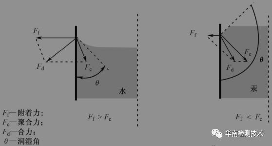
In the above schematic, the liquid molecules are subjected to two forces: adhesive force Ff and cohesive force Fc (ignoring the effect of gravity). Based on the shape of the liquid surface, the external force acting on the liquid surface is perpendicular to the liquid surface. Because the adhesive force between water and the glass wall is greater, the resultant force Fd points towards the inside of the glass wall. Therefore, the resultant force Fd forms a concave surface with the liquid surface at a right angle. When the liquid surface forms a concave shape, due to the action of surface tension, a contraction force is generated, leading to a decrease in pressure on the liquid surface inside the tube. However, the pressure at all points on the same liquid surface must be equal, causing the liquid surface to rise. In short, due to the strong adhesive force between water and the glass wall, the liquid surface presents a concave shape. The reduction in pressure due to surface tension causes the liquid surface to rise.
During the soldering process, wetting and the cohesive forces of molten solder are closely related to the adhesion of the base metal. When the adhesion between solid surfaces and liquid atoms is strong, that is, when the attractive forces at the solid-liquid interface exceed the cohesive forces between liquid molecules, capillary action is likely to occur. In other words, if the adhesion on the solid surface is relatively strong, stronger than the cohesive forces between liquid molecules, the liquid will spread and lay out more easily on the solid surface to form capillary action.
Thus, it can be concluded that to achieve solder joint bonding, the first requirement is to produce a wetting effect. Through the wetting action, when the distance between the atoms of the liquid solder and the base metal is very close, the cohesive forces between the atoms begin to take effect, causing the liquid solder to merge with the base metal, ultimately completing the bonding process.
The connection strength of soldering is achieved by forming an alloy layer at the joint interface. This alloy layer is typically composed of intermetallic compounds. Intermetallic compounds are compounds formed based on the atomic weight ratio of the metal components.
When using Sn-Pb solder to solder copper, Sn and Cu will diffuse into each other, forming a Cu-Sn-Cu bond. This bond generates Cu3Sn (ε phase) on the base metal side at room temperature and Cu6Sn5 (η phase) on the solder side, while at temperatures above 300°C, Cu31Sn8 (γ phase) and other structurally undefined alloy forms may also appear.
Intermetallic compounds are a type of alloy phase with high hardness and brittleness. Due to the strong chemical affinity between Cu and Sn, the intermetallic compounds formed at the soldering joint interface grow rapidly. According to relevant data, the intermetallic compound layer formed by pure Sn reacting with Cu at 265°C in liquid state can reach a thickness of 1.25μm in just one minute.
① The surface of the base metal is not cleaned, and there are oxides, contaminants (such as dirt, grease, sweat stains), leading to poor weldability or even unweldability of the soldering surface.
② PCB and components purchased from outside have not undergone strict weldability acceptance tests before entering the user warehouse, leading to potential soldering issues.
③ Poor storage conditions lead to prolonged inventory periods, which may cause a decline in the performance of soldering materials.
④ The temperature of the soldering pot is too high, causing the solder to oxidize rapidly at the contact surface with the base material, reducing the adhesion of the liquid solder. High temperatures can also corrode the roughness of the base material’s surface, weakening capillary action and deteriorating fluidity.
Prevention of Cold Solder Joint
To ensure that PCBs and components with poor weldability do not enter the warehouse, we must strictly adhere to the incoming inspection procedures.
① Each batch of purchased components must undergo weldability sampling tests according to IPC/J-STD-002 standards upon arrival. Only after passing the tests can they be officially stored.
② Each batch of outsourced PCBs should have three samples randomly selected for weldability testing, conducted according to IPC/J-STD-003 standards. Only after passing the tests can they be accepted. Since PCBs that have undergone weldability testing cannot be reused, three additional pieces should be ordered as process test samples for each batch.
① The storage environment should maintain constant temperature and humidity, with good air quality, free from corrosive gases (such as sulfur, chlorine, etc.) and oil stains. This can effectively prevent oxidation and contamination, maintaining the weldability of component surfaces.
② Considering the storage period of weldability, components must be managed according to the first-in, first-out principle to prevent some components from declining in weldability due to prolonged storage.
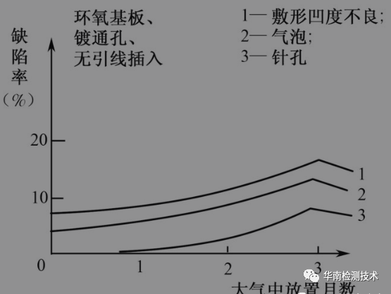
③ The length of storage periods should be determined based on regional and local air quality. Generally, we hope to minimize inventory periods. For example, for PCBs, weldability can significantly deteriorate after being placed in the atmosphere for one month, and they are prone to moisture absorption. For details, please refer to the figure below:
④ Improve storage conditions: For humid and hot environments, especially in Guangzhou, even with vacuum packaging, PCBs should not exceed six months. Consider using dehumidification equipment or setting up humidity control devices in the storage area to ensure suitable environmental humidity.
⑤ For components and PCBs that exceed the storage period, they can only continue to be used after passing the weldability tests and meeting the requirements. This can avoid potential risks of weldability degradation due to prolonged storage.
① Staff should wear anti-static clothing, shoes, and gloves, and keep them clean frequently: To prevent the accumulation and transfer of static electricity, staff should wear anti-static clothing, shoes, and gloves during wave soldering operations. It is also very important to keep these anti-static gear clean.
② Pay attention to remove grease and other organic contaminants: Most fluxes can only remove rust and oxide films, and cannot remove grease and other organic films. If components and PCBs are affected by grease and other contaminants during storage or production, it will lead to a decrease in soldering strength, resulting in issues such as solder and lead segregation and pinholes. In addition, cracks are also likely to occur at the segregation points and solder joint interfaces, which are not detectable by appearance but pose potential threats to reliability. Therefore, any items that come into contact with the soldering surface must remain clean during operations.
③ Use gloves that meet EOS/ESD protection requirements: When removing PCBs, staff should wear gloves that meet EOS/ESD protection requirements and can only touch the corners or edges of the PCBs. This can reduce the impact of factors such as sweat on the solderability of the soldering surface.
① Before soldering, it is essential to clean all surfaces to be soldered to ensure they have good weldability. This includes removing copper chips or other impurities and ensuring surfaces are free of grease, oxides, or other contaminants.
② When we need to consider both the safety and reliability of solder joints, we can select flux with stronger activity according to actual conditions. Such fluxes can better remove oxides and improve the wetting of solder joints, thereby promoting the quality and reliability of soldering.
Definition of Cold Soldering
In the wave soldering joint interface, if wetting occurs but the required diffusion process does not take place, and the formation of the alloy layer (IMC) at the joint interface is not apparent, we can define it as cold soldering. Please refer to the figure below.

Manifestation of Cold Soldering
The surface of a cold solder joint appears to be wetted, but in fact, there is no metallurgical reaction occurring at the interface between the solder and the base metal, thus no appropriate thickness of the alloy layer (IMC) is formed, as shown in the figure below. This phenomenon indicates that there is no issue with the weldability of the PCB and components, while the fundamental reason for this phenomenon is the inappropriate selection of soldering process conditions. This invisible defect phenomenon is not easy to judge by appearance, thus posing a significant hazard.
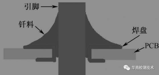
Formation Principle of Cold Soldering
As shown in the figure above, cold soldering mainly refers to the absence of a significant atomic diffusion process at the interface between the molten solder and the base metal. The fundamental reason for this phenomenon can be insufficient heat supply during soldering or too short a contact time with the wave. During the soldering process, atomic diffusion is bidirectional, specifically:
For the dissolution of base metal in solder, it is necessary to meet the condition that the base metal and the liquid solder can dissolve into each other. If this condition is met, the base metal can be dissolved by the liquid solder during the soldering process. At this time, the amount of base metal dissolved in the liquid solder can be expressed by the following formula:
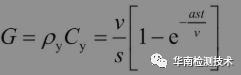
Where
G——Amount of base metal dissolved;
ρy——Density of liquid solder;
Cy——Limit solubility of base metal in liquid solder;
v——Volume of liquid solder;
a——Diffusion coefficient of base metal atoms in liquid solder;
t——Contact time;
s——Contact area between liquid and solid phases.
The effect of temperature on the dissolution amount is mainly reflected in the increase of the solubility coefficient a in the formula, as shown in the figure below.
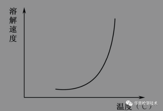
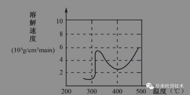
It can be seen that as the soldering temperature increases and the soldering time increases, the amount of base metal dissolved in the liquid solder will increase. However, if intermetallic compounds can form between the solder and the base metal, it will hinder the dissolution rate of the base metal into the solder. On the temperature curve for compound formation, we can see that the dissolution rate will slow down, as shown in the figure below.
During the process of base metal diffusion into the solder, due to the alloying reaction between the base metal elements and the tin (Sn) in the solder composition, the performance of the solder joint is improved. For instance, if a copper-tin alloy layer is formed, the tensile strength (σb) of the solder joint can be increased to 5.7kg², while without the formation of an alloy layer, the tensile strength of tin is only 1.5kg².
However, it should be noted that if the amount of base metal dissolved in the solder is inappropriate (too much), it may lead to adverse consequences, such as increased melting point of the solder, deterioration of solder flowability, and erosion of the base metal. Therefore, careful control of the alloying reaction between the base metal and the solder is necessary during cold soldering to ensure the quality of the solder joint.
According to Fick’s law, at a certain temperature, the amount of diffusion of Sn from the solder components into the base metal is also proportional to the heating time, indicating that the formation of an appropriate alloy layer requires time. Therefore, low soldering temperature and short soldering time are the causes of cold soldering phenomena.
In wave soldering, the main reasons for this phenomenon are:
① Low temperature of the solder pot.
② Excessively fast feeding speed.
③ Poor PCB design. If many component leads with significantly different thermal capacities are soldered at the same time and temperature, it will lead to significant temperature differences at the solder joints of various components. Those with large thermal capacities will absorb insufficient heat and thus be at lower temperatures, leading to deteriorated wetting conditions and the inability to form an ideal alloy layer.
Solutions for Cold Soldering
① Adjust soldering temperature and time.
② Improve PCB design to avoid significant thermal traps during wave soldering.
③ Inappropriate selection of process specifications is a key factor leading to cold soldering phenomena.
Therefore, under the premise of setting the soldering pot temperature at 250°C, it is necessary to ensure that the alloying time is between 3 to 4 seconds.
Non-Wetting and De-Wetting Phenomena
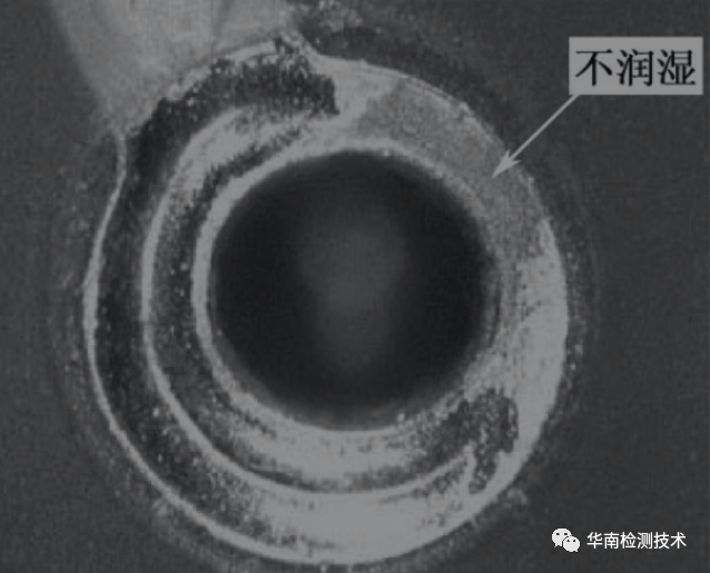
On non-wetting surfaces, the solder does not fully contact the base metal, and thus exposed base metal can be clearly seen, as shown in the figure below.
In wave soldering, the solder first wets the surface of the base metal, but then retracts due to poor wetting, leaving a thin film of solder covering only part of the area of the base metal, while also leaving some separated solder balls. The points of contact between large solder balls and the base metal have large contact angles, and the shape of the solder is irregular, as shown in the figure below.

Formation Principle of Non-Wetting and De-Wetting
① Base metal is unweldable.
② The activity of the flux used is insufficient or the flux has degraded and failed.
③ Oil or grease on the surface prevents the flux and solder from contacting the soldering surface.
① A certain form of contamination on the base metal surface causes semi-wetting phenomena.
② When the concentration of metal impurities in the solder pot reaches a certain level, a de-wetting state may also occur.
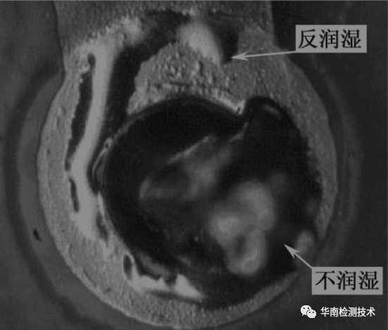
③ In extreme cases of severe contamination leading to poor weldability, non-wetting and de-wetting may coexist on the same surface, as shown in the figure below.
④ Improper control of soldering time and temperature may lead to excessively thick interfacial alloy layers, resulting in de-wetting phenomena.
Solutions for Non-Wetting and De-Wetting
① Improve the weldability of the base metal.
② Select a flux with stronger activity as appropriate.
③ Reasonably adjust soldering temperature and time.
④ Thoroughly remove oil, grease, and organic contaminants from the surface of the base metal.
⑤ Maintain the purity of solder in the solder pot.
Testing Process
1. Determine the testing items, conditions, and standards;
2. Sales personnel provide test quotations based on the experimental outline;
3. Sign a commissioned testing agreement, clarifying the unit name, product name, testing items, etc.;
4. The client pays the testing fee, and the testing engineer arranges the test schedule;
5. After determining the testing date, the client sends samples;
6. The commissioned agreement is entered into the system, and a specialized testing engineer is assigned to conduct the tests;
7. After passing the tests, a testing report is issued within five working days;
8. An electronic or paper version of the Chinese testing report is provided.
Chip Identification, Chip Screening, Composition Analysis
Reliability Testing, Automotive AEC-Q Certification
Fair, Efficient, Accurate, Reliable, Reasonable Costs

Official Website: www.gdhnjc.com
Service Hotline: 0769-82186416
Contact Number: 139-2686-7016
Email Address: [email protected]