What is a shift register?
In FPGA (or ASIC), a shift register is a very common basic module. Its essence is to connect multiple flip-flops (registers) in a chain.
All flip-flops share the same clock signal, and the output of each flip-flop is connected to the input of the next flip-flop. In this way, data is “passed” step by step with each clock cycle.
The main uses of shift registers are threefold:
-
Data Delay — Delaying the time at which data appears in the circuit.
-
Serial to Parallel — Combining incoming data bit by bit into a multi-bit byte.
-
Parallel to Serial — Outputting a byte of data bit by bit.
Implementing Delay with Shift Registers
This is the most common application. For example, if you want to delay data by 4 clock cycles before using it, you can connect 4 flip-flops in series. This way, the input data must go through 4 clock transitions before it is output from the last flip-flop.
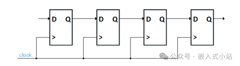
Simple Understanding: It’s like a relay race where the person in front passes the ball to the person behind them, and after 4 passes, the ball reaches the last person.
In VHDL or Verilog, you only need to write a few lines of code to achieve this delay function.
VHDL Implementation
-- Define a 4-bit shift register
signal r_Shift : std_logic_vector(3 downto 0);
process (i_clock)
begin
  if rising_edge(i_clock) then
    r_Shift(3 downto 1) <= r_Shift(2 downto 0); -- Shift left by one bit
    r_Shift(0) <= i_Data_To_Delay;     -- New data enters the lowest bit
    -- The data in the 3rd bit is effectively delayed by 4 clock cycles
  end if;
end process;
Verilog Implementation
// Define a 4-bit shift register
reg [3:0] r_Shift;
always @ (posedge i_clock)
begin
  r_Shift[3:1] <= r_Shift[2:0];  // Shift left by one bit
  r_Shift[0] <= i_Data_To_Delay; // New data enters the lowest bit
  // The data in the 3rd bit is delayed by 4 clock cycles
end
The input data first enters the lowest bit, and then shifts left by one bit with each clock cycle. Finally, when outputting from the 3rd bit, it is equivalent to being delayed by 4 clock cycles.
Serial to Parallel
When data comes in bit by bit (for example, from a UART receiver), you need to combine them into a byte for use. Shift registers can do just that.
For example: UART transmits 8 bits of data (1 byte) at a time, with data coming in one bit at a time in order. The shift register will place the new bit in each clock cycle and shift the existing data back. Once all 8 bits are received, you have a complete byte.
VHDL Implementation
signal r_RX_Data   : std_logic := '0';              -- Current received bit of data
signal r_Bit_Index : integer range 0 to 7 := 0;     -- Bit counter (total 8 bits)
signal r_RX_Byte   : std_logic_vector(7 downto 0);  -- Received complete byte

p_UART_RX : process (i_Clk)
begin
  if rising_edge(i_Clk) then
    r_Rx_Byte(7) <= r_Rx_Data;         -- New data placed in the highest bit
    r_Rx_Byte(6 downto 0) <= r_Rx_Byte(7 downto 1); -- Shift right
    -- Equivalent to: r_RX_Byte(r_Bit_Index) <= r_RX_Data;
    if r_Bit_Index < 7 then
      r_Bit_Index <= r_Bit_Index + 1;    -- Not yet finished receiving 8 bits
    else
      r_Bit_Index <= 0;                  -- 8 bits received, one byte completed
    end if;
  end if;
end process;
Verilog Implementation
reg       r_Rx_Data   = 1'b1;   // Current received bit of data
reg [2:0] r_Bit_Index = 0;      // Bit counter (0-7)
reg [7:0] r_Rx_Byte   = 0;      // Store the received complete byte

always @(posedge i_Clock)
begin
  r_Rx_Byte[7] <= r_Rx_Data;     // New data placed in the highest bit
  r_Rx_Byte[6:0] <= r_Rx_Byte[7:1]; // Shift right
  // Equivalent to: r_Rx_Byte[r_Bit_Index] <= r_Rx_Data;
  if (r_Bit_Index < 7)
    r_Bit_Index <= r_Bit_Index + 1; // Continue receiving
  else
    r_Bit_Index <= 0;               // 8 bits received, one byte completed
end
Each time a new bit of data arrives, it is placed in the highest bit of the byte, and the existing data shifts right until all 8 bits are received. This way, serial data is combined into a complete byte.
Parallel to Serial
This is the reverse operation of the above, commonly found in UART transmitters. You have a byte of data to send out, but UART can only send one bit at a time. Shift registers can help you output this byte bit by bit.
For example: the least significant bit (LSB) of the byte is sent first, and the remaining bits shift back until all bits are sent out.
VHDL Implementation
signal r_Bit_Index : integer range 0 to 7 := 0;     -- Bit counter
signal r_TX_Data   : std_logic_vector(7 downto 0);  -- Byte to be sent

p_UART_TX : process (i_Clk)
begin
  if rising_edge(i_Clk) then
    o_TX_Serial <= r_TX_Data(0);                   -- Send the least significant bit first
    r_TX_Data(6 downto 0) <= r_TX_Data(7 downto 1);-- Shift right
    -- Equivalent to: o_TX_Serial <= r_TX_Data(r_Bit_Index);
    if r_Bit_Index < 7 then
      r_Bit_Index <= r_Bit_Index + 1;              -- Continue sending
    else
      r_Bit_Index <= 0;                            -- Sending completed
    end if;
  end if;
end process;
Verilog Implementation
reg [2:0] r_Bit_Index = 0;  // Bit counter
reg [7:0] r_Tx_Data   = 0;  // Byte to be sent

always @(posedge i_Clock)
begin
  o_TX_Serial <= r_TX_Data[0];   // Send the least significant bit first
  r_TX_Data[6:0] <= r_TX_Data[7:1]; // Shift right
  // Equivalent to: o_TX_Serial <= r_Tx_Data[r_Bit_Index];
  if (r_Bit_Index < 7)
    r_Bit_Index <= r_Bit_Index + 1; // Continue sending
  else
    r_Bit_Index <= 0;               // Sending completed
end
The data to be sent is first placed in the register, and each clock cycle, the least significant bit is sent out first, then the entire byte shifts right until all 8 bits are sent.
Conclusion
Shift registers are commonly used in FPGA or ASIC, and they can:
-
Control data delay,
-
Convert between serial and parallel data.
Understanding them is like understanding the process of a “passing relay” where each flip-flop is a person, and the data is like a relay baton, continuously passed along with the clock’s rhythm.