Commercial off-the-shelf FPGAs are considered the only way to meet the increasing processing power demands of space applications. Due to their sensitivity to multi-bit flips, specialized design hardening techniques are required to address single particle effects in space applications. A fault-tolerant technology framework based on three levels: user logic layer, configuration memory layer, and control layer is proposed. In the user logic layer, a novel low-overhead FTR strategy is introduced for error detection in user logic; at the configuration memory level, a dynamic partial reconfiguration strategy based on modules and frames is proposed to handle errors in configuration memory; at the control level, targeting the Xilinx ZYNQ System-on-Chip FPGA, the embedded hard processor is utilized for circuit state saving and recovery based on checkpointing and rollback mechanisms. The entire fault-tolerant technology framework was experimentally validated through fault injection tests conducted on the LEON3 open-source processor with a 7-stage pipeline, showing that 99.997% of injected faults were promptly corrected under conditions of increased usage of 85% LUT resources and 125% flip-flop resources.
0 Introduction
Commercial chips have stronger processing capabilities than space-grade chips but are more susceptible to single particle effects[1-2]. Many scholars have conducted related research, mainly to mitigate erroneous data bits in configuration memory through continuous global configuration refreshing[3]. Based on this, reference [4] proposed a dynamic partial reconfiguration (DPR) technology to reconfigure specific circuit areas, which reduces configuration time and improves efficiency.
Another feasible approach is to perform error detection and correction coding within the configuration memory, which can typically detect 2-bit errors and correct 1-bit errors (Single Error Correction and Double-Error Detection, SEC-DED) but cannot handle multiple bit upset (Multiple bit Upset, MBU) situations[5]. There are mainly two ways to design fault tolerance for user logic circuits: one is to perform triple modular redundancy (Triple Modular Redundancy, TMR) design, which has a significant cost disadvantage; the other method is to only perform error detection in the user logic circuit using duplication with comparison (Duplication With Comparison, DWC) technology, where all logic resources are duplicated, and comparators are added to compare results. To further reduce resource utilization, reference [6] proposed to perform error detection in the user logic circuit while adding another layer for circuit state saving and recovery.
Based on the above analysis, current soft error technologies for FPGAs mainly involve the user logic layer, configuration memory layer, and control layer. Different technologies can target different scenarios, but there is no targeted optimization for specific applications regarding resource and power consumption. Therefore, this paper proposes a systematic framework for mitigating the MBU problem in FPGAs based on a low-overhead three-level design, and simulative validation through fault injection on the Xilinx ZYNQ platform targeting the open-source LEON3 processor is provided.
1 Three-Level Soft Error Mitigation Technology Framework
With the optimization goals of minimal resource overhead, lowest power consumption, and shortest processing delay, a systematic soft error mitigation technology framework is proposed to address the MBU capability issues faced by commercial off-the-shelf FPGAs in space applications through effective collaboration among the user logic layer, configuration memory layer, and control layer. The fault-tolerant technology framework based on the Xilinx ZYNQ SoC (System-on-Chip) is shown in Figure 1.
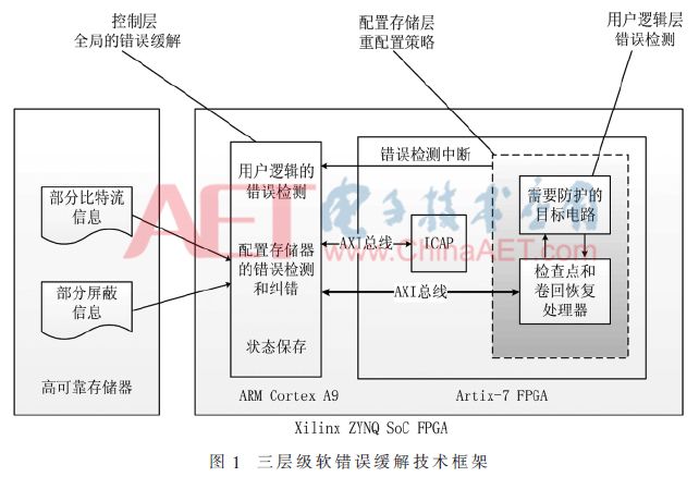
The redundancy strategy selected at the user logic layer directly impacts the architecture of the upper layers. For example, using TMR technology for soft error mitigation requires over 200% resource overhead, which is not suitable for space application environments with strict resource and power limitations. The optimization goals need to focus on reducing area and power consumption while minimizing delays.
The delay and power consumption of the strategy chosen at the configuration memory layer mainly depend on the granularity of reconfiguration and error correction capability, which in turn depends on whether the entire configuration data or only the built-in error correction code redundancy information is read and written back.
In the control layer, the main factors considered are also delay and power consumption. Checkpointing and rollback mechanisms can be employed, with the primary design parameter being the period for setting checkpoints.
2 User Logic Layer
In the user logic layer, two more common error detection methods are: one is DWC technology, a fully hardware backup strategy; the other is temporal redundancy (Temporal Redundancy, TR) technology. The combinational and sequential logic in Figure 2 has two independent paths, allowing for comparison at each flip-flop output, thus minimizing detection delay. Figure 3 employs a TR technology system, where only sequential logic is redundant, typically using one clock for the basic circuit and another delayed clock providing redundancy to the flip-flops, keeping the worst-case hold time constraint at d while the setup time constraint remains unchanged. This strategy can be used to detect single particle flips in sequential logic and single-event transients (SET) in combinational logic with minimal resource overhead.
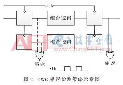
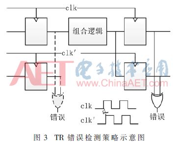
The delay time d must first ensure that all SETs in combinational logic can be detected, thus it must be greater than the maximum duration of SET. As technology nodes shrink, SET durations are increasing. For a LET of 30 MeV·cm2/mg and a 130 nm process, the SET duration is 0.2–0.8 ns, while the Xilinx ZYNQ uses a 28 nm technology, with a delay of around 2 ns. Moreover, as delay d increases, more delay wiring resources need to be added, which can easily cause race hazard phenomena, greatly reducing the maximum clock operating frequency. Therefore, for delays up to 2 ns, the use of TR strategies is severely limited.
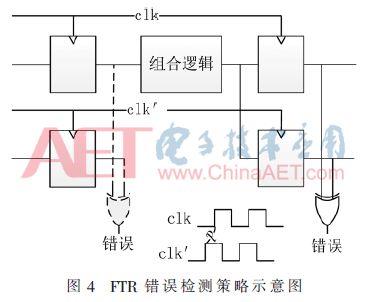
To improve the applicability of the TR strategy, a forward temporal redundancy (Forward Temporal Redundancy, FTR) strategy is proposed as shown in Figure 4, where the main difference from TR is that the delay is reversed. The clock phase used for flip-flop comparison is advanced, keeping the circuit’s hold time unchanged but making the setup time constraints more stringent. Therefore, the maximum propagation delay from clk to clk′ clock domains is reduced by d. FTR is a low-power and low-area solution that avoids race conditions.
3 Configuration Memory Layer
For the reconstruction or refresh of configuration memory, there are mainly three different granular operations, as shown in Figure 5. The first is complete reconfiguration or refresh, which is less efficient; the second is module-based partial reconfiguration, suitable for circuits confined to partially reconfigurable regions (Partially Reconfigurable Region, PRR); the third is the best operational granularity, which is frame-based partial reconfiguration. A frame is the minimum unit based on an address table, and for the Xilinx ZYNQ platform, it includes 101 32-bit words, with each frame accessed via its corresponding Frame Address Register (FAR), providing the fastest error detection capability.
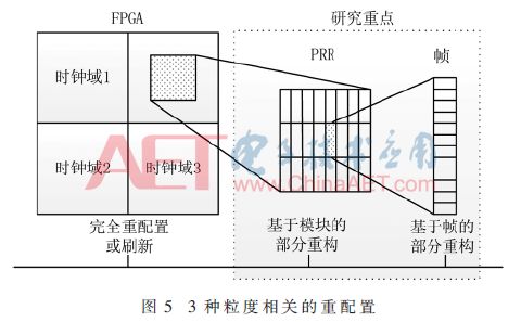
To improve error detection and correction efficiency, a combination of module-based and frame-based DPR methods is proposed at the configuration memory layer: first, accurately locate the resource positions of the user logic circuit while extracting the corresponding bitstream information, and then achieve rapid error detection. Frame-based read-back can be used to detect all errors within the PRR. The bitstream signal includes not only configuration bits but also user memory units, which may change state during circuit operation. These corresponding bits must be masked during read-back using a .mask file.
The above methods are particularly suitable for cases where the user circuit can be divided into several independent small PRRs. The more accurate the area location, the smaller the PRR, the less delay, and the more stable the circuit’s performance.
Meanwhile, hardware error handling can be achieved through bitstream relocation technology, requiring only a small-capacity external memory to store part of the bitstream.
Another common configuration memory protection strategy is the IP core provided by Xilinx, which monitors and corrects errors in the entire configuration memory. This core requires 900 lookup tables and 700 flip-flops without fault-tolerant design in the Xilinx ZYNQ, resulting in significant resource overhead.
Xilinx FPGAs support various refresh and configuration paths. To minimize delays and improve system reliability, the ICAP interface is preferred.
4 Control Layer
The control layer mainly completes two tasks: coordinating processing and state saving. The coordinating processing function is divided into two parts: one related to the user logic layer to handle errors detected in the user logic; the other related to the configuration storage layer to correct errors in the configuration memory. State saving is specifically for supporting checkpointing and rollback operations, as shown in Figure 6, which describes the complete algorithm based on the Xilinx ZYNQ platform.
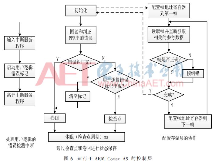
Checkpointing and rollback operations can be implemented in three ways. The first is to use the FPGA’s BRAM to store state information. To ensure that this information is not altered, appropriate protection mechanisms must be employed, usually employing built-in SEC-DED-EDAC, which cannot address MBU situations. The second method involves processing at a higher layer, using read-back capture features to directly retrieve state information from the configuration logic units via the processor. However, this method requires specialized layout design; otherwise, it may incur significant delay overhead. The final method is to transmit via internal data buses, such as AXI, which can be shared in multi-PRR module designs. Similar to the second method, the retrieved state data can be corrected using software encoding with higher error correction capabilities or stored in single particle immune memory to ensure data correctness, which can also be returned to support rollback operations.
Based on the trade-off between delay and power consumption, an optimized checkpoint period parameter is selected. The processor executes tasks according to a time cycle, which needs to be adjusted based on application requirements. For hard real-time systems, the checkpoint period can be reduced to zero, with the minimum delay bound determined by the read-back time. Using a hard processor for control reduces the use of FPGA resources sensitive to single particles, improving the overall reliability of the system.
5 Test Results Using Open-Source LEON3 Processor Core
This paper uses the open-source LEON3 processor soft core as the basic program for testing. Its state units mainly include the program counter, register file, and data memory, which need to be protected through checkpointing and rollback operations. Testing is conducted based on the Xilinx ZYNQ XC7Z010-1CLG400C platform.
In the user logic layer, a quantitative comparison of different redundancy strategies is conducted, with the results shown in Table 1. As can be seen from the table, the FTR strategy yields the best results, with low power consumption and low area overhead, making it suitable for space applications, achieving the best balance between performance and cost. Due to the stricter setup time constraints, the FTR strategy can operate at a higher maximum working frequency compared to TR.
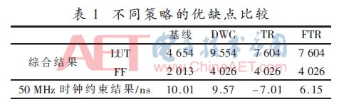
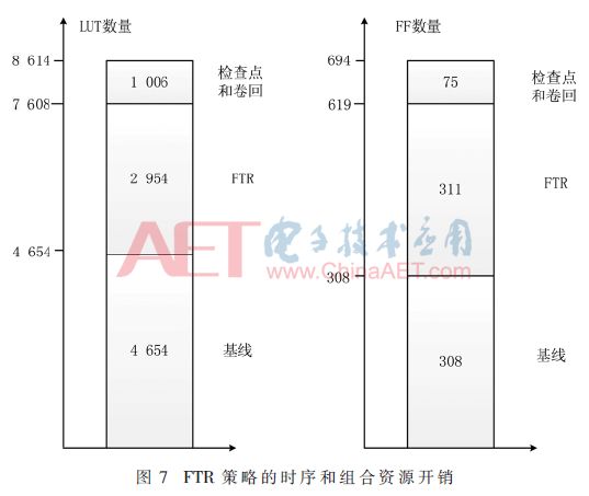
Figure 7 shows the resource overhead required for implementing all mitigation techniques. It can be seen that using the FTR strategy only increased the combinational logic and sequential logic resources by 63% and 101%, respectively.
In the configuration memory layer, more accurate positioning reflects the advantages of FTR, requiring only 34 μs to correct an error in a frame. The LEON3 processor includes 2,640 frames, allowing for the entire PRR read-back within 90 ms. Further speed optimization of the ICAP port can reduce this time, with a maximum operating frequency of up to 300 MHz.
In the control layer, state information is stored in the program counter, register file, and data memory, protected through checkpointing and rollback operations and connected to the hard processor via the AXI bus. This strategy is sensitive to the amount of data that needs to be transmitted; typically, on-chip data memory only has a few KB, and larger capacity requirements are provided by external memory, which can employ complex error correction coding.
Figure 8 shows that 22% of combinational logic and 24% of sequential logic overhead is used for checkpointing and rollback processing.
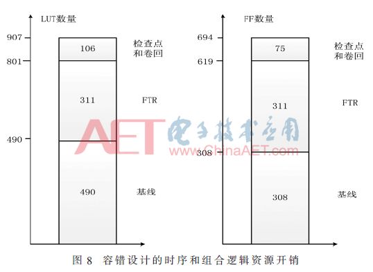
The effectiveness of the entire software mitigation technology framework was validated through fault injection. First, the address information corresponding to the frame was read, then one bit was flipped, and finally, the frame data was written back, resulting in an error. Using the .ebd and .ll files generated by Xilinx, valid bit information can be identified, and experimental results indicate that 99.997% of injected soft errors were corrected.
6 Conclusion
To meet the area and power consumption requirements of low-cost, high-performance space application processing platforms, a three-level optimization model targeting power consumption, area, reliability, and delay characteristics is proposed. Using the LEON3 open-source processor soft core as the benchmark program, redundancy and state preservation were achieved with an increase of 85% in combinational logic and 125% in sequential logic resource overhead, which is superior to the pure DWC system. Through fault injection simulation experiments, it was verified that this framework can effectively correct 99.997% of soft errors and has the ability to mitigate MBU.

References
[1] Feng Xing, Wang Daming, Zhang Yankui, et al. Research on SEU Sensitivity Based on SRAM-type FPGA [J]. Electronic Technology Application, 2016, 42(5): 53-56.
[2] Quinn H, Graham P, Krone J, et al. Radiation-induced multi-bit upsets in SRAM-based FPGAs [J]. IEEE Transactions on Nuclear Science, 2005, 52(6): 2455-2461.
[3] Berg M, Poivey C, Petrick D, et al. Effectiveness of internal vs. external SEU scrubbing mitigation strategies in a Xilinx FPGA: design, test, and analysis [C]. Proceedings of Radiation and Its Effects on Components and Systems (RADECS), 2007: 1-8.
[4] Straka M, Kastil J, Kotasek Z. Fault tolerant structure for SRAM based FPGA via partial dynamic reconfiguration [C]. Proceedings of IEEE Euromicro Conference on Digital System Design: Architectures, Methods and Tools (DSD), 2010: 365-372.
[5] Pradhan D K, Vaidya N H. Roll-forward and rollback recovery performance-reliability trade-off [J]. IEEE Transactions on Computers, 1997, 46(3): 372-378.
[6] Xapsos M A, Stauffer C, Jordan T, et al. Model for cumulative solar heavy ion energy and linear energy transfer spectra [C]. IEEE Transactions on Nuclear Science, 2007, 54(6): 1985-1989.
Author Information:
Zhang Xiaolin, Ding Lei, Gu Liming
(China Electronics Technology Group Corporation, 36th Research Institute, Jiaxing 314033, Zhejiang)