Click the blue text to follow us 1Introduction
PHS resin is a high-performance photosensitive resin specifically designed for deep ultraviolet (DUV) photoresists, widely used in the lithography process of semiconductor chip manufacturing. Its core advantages include high purity, high resolution, and excellent thermal and chemical stability, which can meet the stringent requirements for high precision and reliability in semiconductor production, significantly enhancing the imaging quality and process stability of photoresists during the chip patterning process. Additionally, PHS resin can also be used in various fields such as electronic packaging materials, coatings, and adhesives.
2PHS Resin
In the precise “sculpting” of the microscopic world of chip manufacturing, the lithography process is undoubtedly a key factor determining success or failure. Among them, a high-performance photosensitive resin called PHS resin is becoming the core material of DUV lithography technology due to its outstanding performance.
Excellence in Detail: The Outstanding Performance of PHS Resin
As a key component of DUV photoresists, PHS resin plays an irreplaceable role in the semiconductor manufacturing field due to its high purity, high resolution, and excellent thermal and chemical stability. In the complex process of chip patterning, this material can meet the extreme requirements for precision and reliability in modern semiconductor manufacturing, significantly improving imaging quality and process stability, safeguarding chip performance.
Concentrated Production Capacity and High Technical Barriers
The production of PHS resin has a high technical threshold, with global capacity mainly concentrated in a few large chemical companies in Japan, the United States, and South Korea. These companies have established technical barriers in key parameters such as purity control and molecular weight distribution through years of technological accumulation. In recent years, several Chinese companies have also been actively laying out PHS resin production lines, and some domestic manufacturers have achieved technological breakthroughs and entered the capacity construction stage. However, overall, domestic capacity still cannot meet market demand, and high-end products remain reliant on imports.
Wide Applications, Showcasing Versatility
In addition to its core application in photoresists, PHS resin also demonstrates diverse application potential. In fields such as electronic packaging materials, coatings, and adhesives, it also performs excellently, becoming a “jack of all trades” in high-end manufacturing.
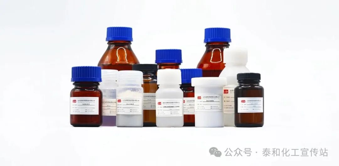
Precise Technical Specifications Ensure Product Quality
PHS resin is produced strictly according to technical standards, with a pale yellow transparent liquid appearance and a solid content of no less than 35.0%. The product is available in two specifications: Specification-1 has a weight-average molecular weight of 10000±2000 and a molecular weight distribution width of ≤1.55; Specification-2 has a weight-average molecular weight of 14000±1000 and a molecular weight distribution width of ≤1.25. The single metal ion content for both specifications is strictly controlled to be below 10 ppb.
Customized Services to Meet Individual Needs
It is worth mentioning that PHS resin supports personalized customization according to customer requirements, whether it is molecular structure, molecular weight, or metal impurity content, adjustments can be made according to specific needs, providing precise solutions for different application scenarios.
Wide Applications and Promising Prospects
In addition to its core application in semiconductor photoresists, PHS resin can also be used in electronic packaging materials, coatings, and adhesives, showing good application prospects. In terms of packaging and storage, PHS resin is typically packaged in electronic-grade plastic barrels, with each barrel weighing 1kg, 2kg, 5kg, 10kg, or 20kg, customizable according to customer needs. It is important to note that this product should be stored in a cool place, avoiding direct sunlight and heat sources, with a general storage period of 12 months. During operation, attention should be paid to labor protection to avoid direct contact with skin and eyes, and in case of contact, rinse thoroughly with plenty of water.
With the continuous development of new technologies such as 5G, artificial intelligence, and the Internet of Things, the semiconductor industry is continuously evolving, and PHS resin, as one of the key materials, will increasingly highlight its strategic position. Domestic upstream and downstream enterprises in the industry chain are strengthening cooperation to jointly promote the localization process of this important material, laying the foundation for the self-controllability of China’s semiconductor industry.
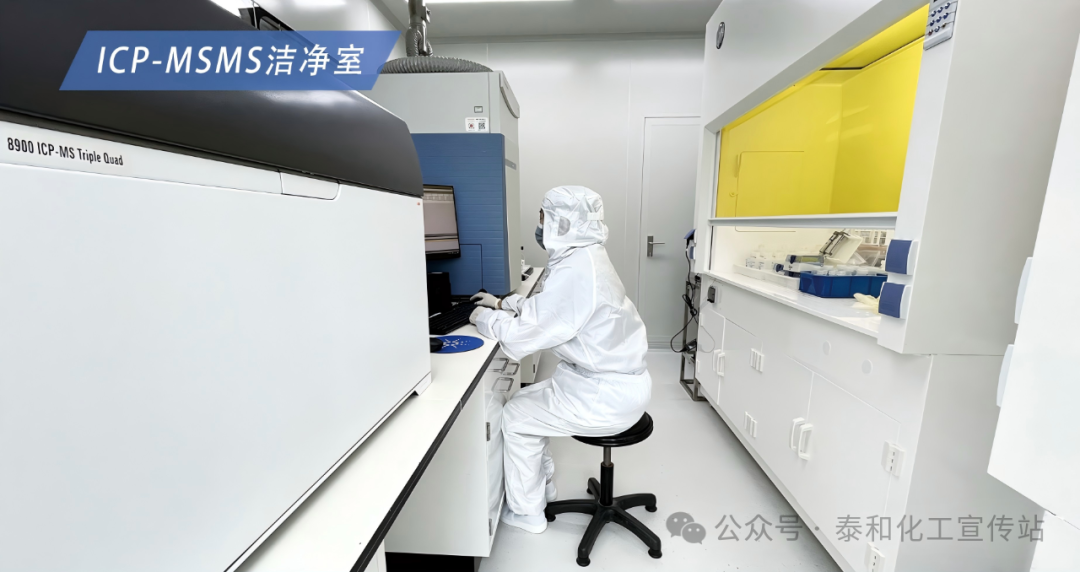
With the continuous advancement of semiconductor technology, PHS resin, as a key material in the lithography process, will continue to contribute significantly to the development of the chip industry. In this invisible microscopic world, it silently safeguards the precision manufacturing of every chip.
If you have any other questions about PHS resin, such as specific preparation process details or practical skills in different application scenarios, feel free to leave a message in the comments section for us to discuss.

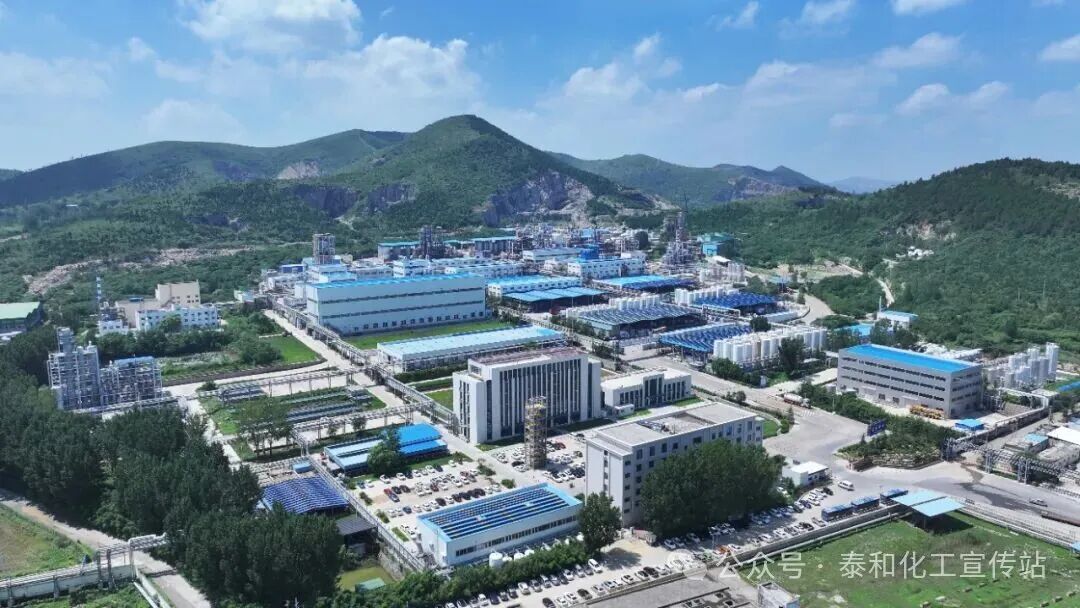
 3Introduction to Taihe Technology
Taihe Technology is a specialized manufacturer of fine chemicals. Through years of continuous R&D investment and technological innovation, it has ensured stable product quality with unique continuous, automated, and unmanned production facilities, reduced energy consumption, and achieved inherent safety; relying on its self-developed information management system, it timely and accurately meets customers’ personalized needs; with strong production capacity and strategic partnerships with suppliers, it guarantees a continuous and stable supply for the entire industry.
Welcome to Collaborate
Website: www.thwater.com
Contact: 0632-5113088
Address: No. 1, Shiliquan East Road, Shizhong District, Zaozhuang City, Shandong Province