 Click the blue text to follow us
  01
01
Analog and RF
01 What is Analog
Analog Signals: In timing and amplifiers, all signals in the continuous natural domain are analog signals; while digital signals are artificially defined and only appear in computers.
Analog Functions:
① amplify
② filter
③ transfer
Classification of Analog: Power supply, AD, DA, PLL, RF, etc.
◐
Academia (UCB/Stanford/MIT/Oregon/TSU/FDU/UESTC, etc.) focuses on “new ideas” for publishing papers and pays less attention to cost, PVT, etc.
Industry (Huawei, ADI, TI, Maxim, ST, Infineon, Goodix, Fudan Micro, Beiling, etc.) is market-driven, and innovation is only to solve problems.
02 Software and Textbooks Required for Learning Analog
Software:
① Circuit design, layout, and simulation: Cadence
② Document writing: Visio
③ Modeling and simulation: Matlab
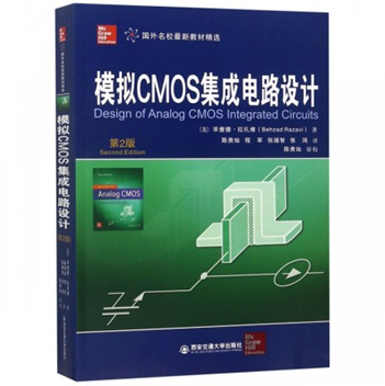 Introductory Book: Razavi
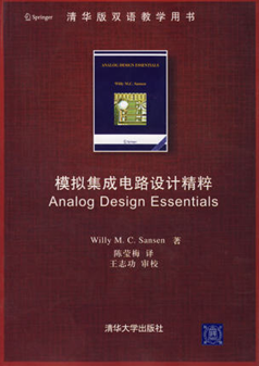 Advanced Book: Sansen
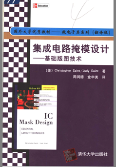 Layout Book: Integrated Circuit Mask Design03 Software and Textbooks Required for Learning RF
Software:
① Circuit design, layout, and simulation:Cadence
② Electromagnetic field simulation:ADS Momentum/HFSS, mainly used for simulating inductors and transmission lines.
③ System modeling and simulation:Matlab (including Simulink)/ADS
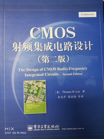 Introductory Book: CMOS RF Integrated Circuit Design (Second Edition)Benefit: There is a translated version, easy to understand for beginners.
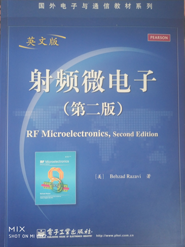
Advanced Book: RF Microelectronics (Second Edition)
Review: A professional book, but very difficult to digest; I haven’t finished reading it..
Auxiliary Books: Books related to Signal and Systems or Digital Signal Processing Experience Summary: People engaged in RF must understandSignal and Systems, otherwise it is difficult to have a deep understanding of RF.
04 RF Directions
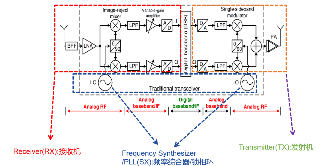
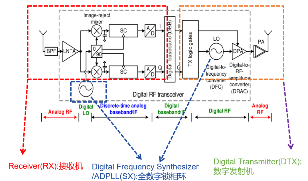
05 RF Related Companies
RF Company Classification:
1.IoT (Internet of Things): Low power consumption, medium performance requirements. 2.Communication Chips: 5G chips, soon 6G, high performance. 3.Millimeter Wave Radar Chips: Ultra-high frequency, automotive radar, smart parking, very popular in recent years.
Examples of Companies:
Huawei HiSilicon: RF has many departments, it’s best to inquire before going. Generally, they make chips for Huawei products. ASR (Aojie): Mobile communication chips. Verisilicon (Chip Original): IoT chip IP. RDA, Hengxuan (wireless headphones), Fudan Microelectronics (IoT) Currently, there are many startups in IoT and millimeter wave radar; keep an eye on them~
06 Development Trajectory of Analog and RF
① Engineers: Technical route, specializing in a certain circuit, such as PLL, then gradually expanding to other circuits.
② System Engineers: Familiar with signals and systems, understand circuits for receivers, transmitters, and phase-locked loops, not necessarily in-depth. This role generally formulates system architecture and specifications, and it is difficult for fresh graduates to take on; a PhD may be possible with certain work experience, but it is not advisable for freshly graduated PhDs due to lack of experience.
③ Management Positions: Project leader, leading project teams, also needs to understand certain systems and circuits, planning progress and evaluating projects. It is difficult for fresh graduates to take on; certain work experience is required.
02
Devices and Processes
01 Course Setup and Characteristics
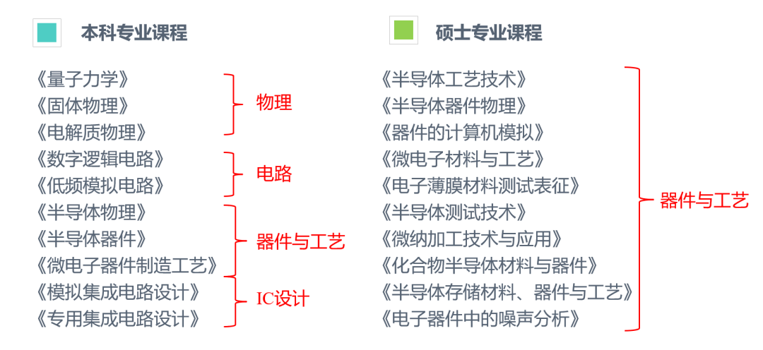
Master’s Course Characteristics:
Meetsdegree foundation courses,degree major courses and professional elective courses credit requirements, allows students to freely choose courses they wish to study, including IC design courses. Some courses have midterm and final closed-book exams, while others only require assignment submissions.
Diverse Forms, may require students to present part of the content, or the teacher may not hold classes, requiring students to read papers independently.
The vast majority of courses will be completed in the first year of the master’s program; generally, there are no classes in the second and third years.
02 Research Directions
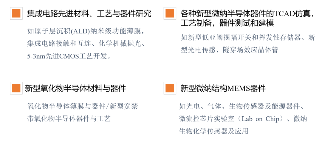
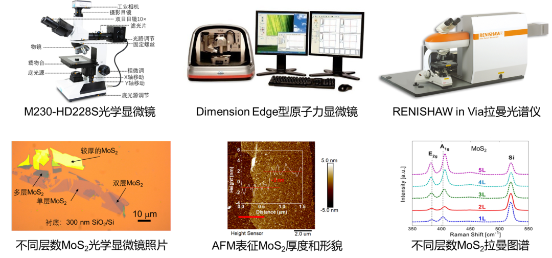
Wafer-level two-dimensional semiconductor materials, devices, and their circuit applications / low-dimensional electronic materials and devices / research on nano-devices and processes, research on new nano-devices, growth of low-dimensional semiconductor materials / properties of materials, device processes, and other basic and application fields.
Research on new two-dimensional layered semiconductor electronic devices and characteristics
Controlled growth of wafer-level two-dimensional semiconductors, device processes, circuit design, and their practical applications in integrated circuits, including logic, storage, and RF devices.

03
Research Conditions and Employment
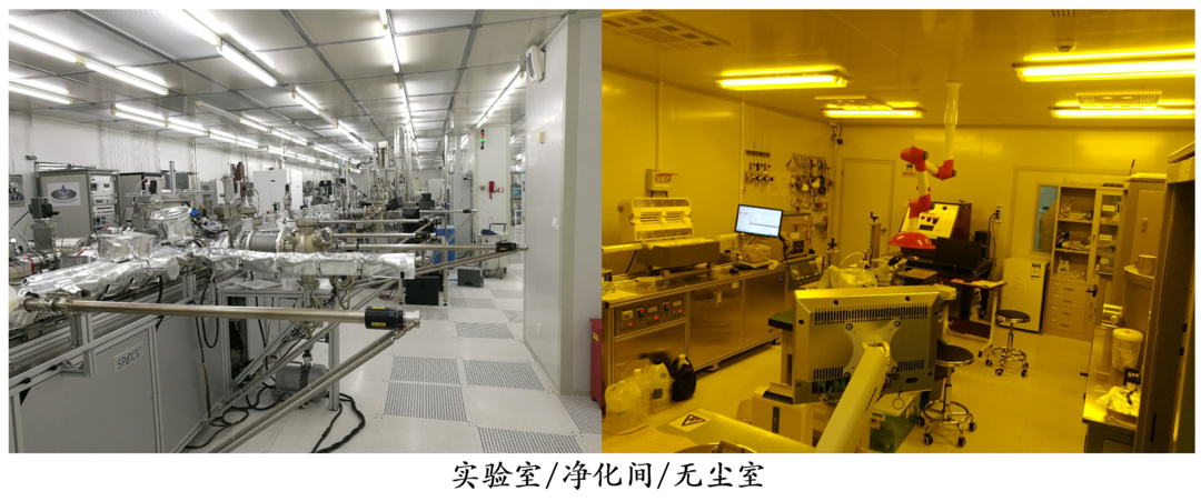
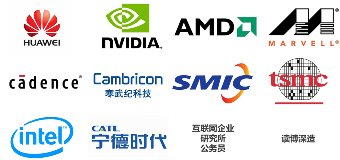
Chooseenterprises related to the major, for example, there are relatively few master’s graduates going to Fab plants.
The majority choose IC design companies and positions, or go to internet companies, where there are many job opportunities, high demand, and high salaries.
Employment direction and job positions are not absolutely related to the major and research direction.
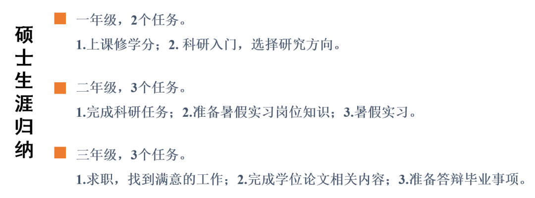
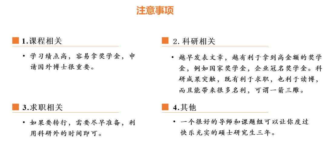
04 Summary and Precautions
03
FPGA Direction
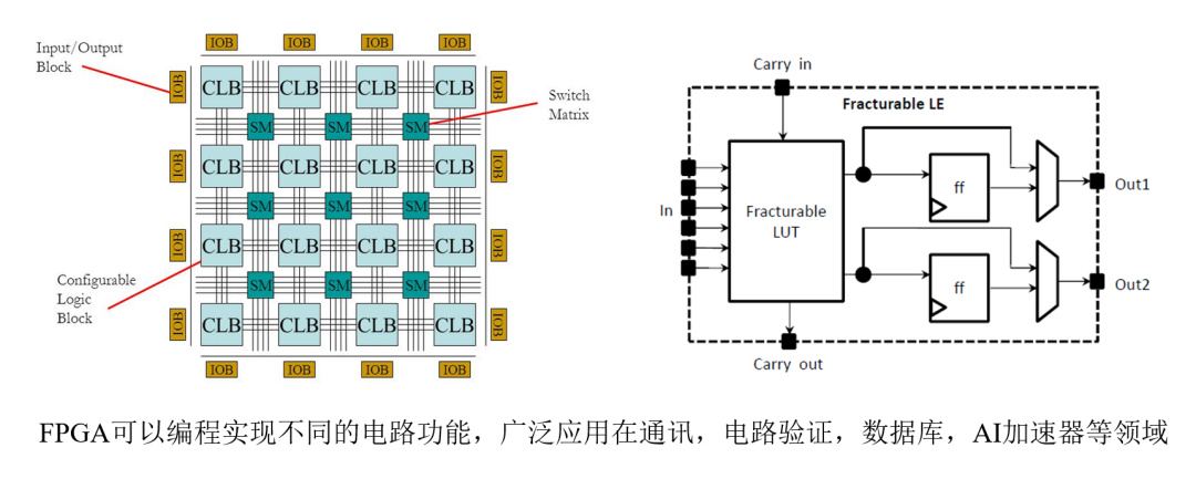
01 FPGA Chips
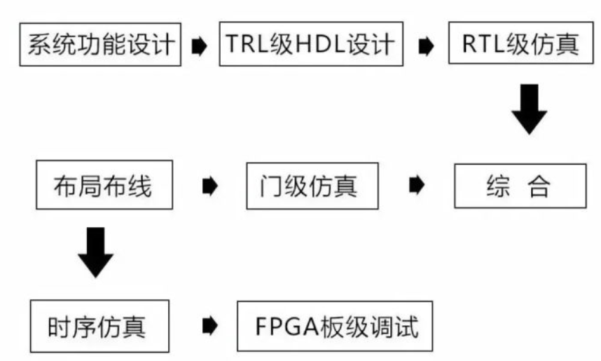
Usage Process:
Current Situation at Home and Abroad:
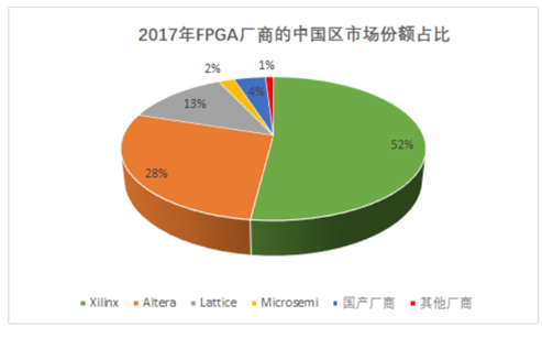
Two giants abroad: Xilinx and Intel Altera department
Domestic companies: Fudan Microelectronics, Shanghai Anlu, Shenzhen Ziguang Tongchuang, Guangdong Gaoyun
Research institutions at home and abroad: University of Toronto, Chinese University of Hong Kong, Chinese Academy of Sciences, Tsinghua University, Fudan University.
The domestic FPGA market size is approximately10 billion, and the trade war has spurred the development of domestic FPGA.
02 Research Directions
Direction 1: FPGA Chip Design
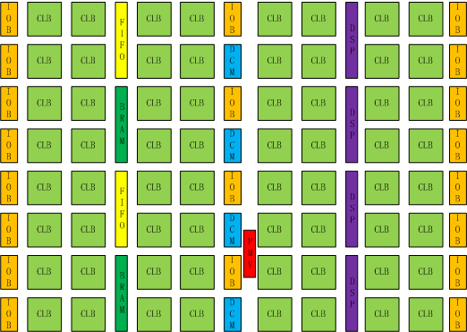
FPGA itself is a chip, containing manycircuit modules, CLB, IO; BRAM, DSP, FIFO; AI cores, CPU cores, etc.
FPGA itself is a chip, mostly digital modules CLB, BRAM, DSP, etc., with a small portion being IO, PLL and other analog circuit modules.
FPGA module design has specialpower, timing, area and other requirements.
Direction 2: FPGA CAD Software
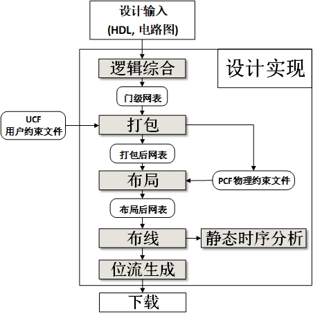
Synthesis: Transforming Verilog into LUT-level units
Packing: Aggregating LUT-level units into CLB-level units
Placement: Placing used CLB units onto the FPGA array
Routing: Determining connection paths between units
Direction 3: FPGA Applications
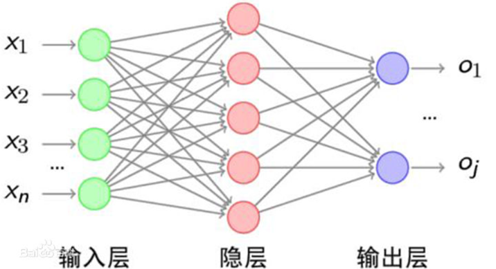
Most popular application:Deep Learning Accelerator
03 Employment Aspects
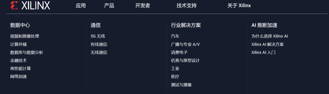
Applications Equal Employment!
04
Digital Direction
01 Digital IC Design Process
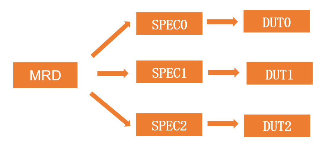
Front-end:

Mid-end:
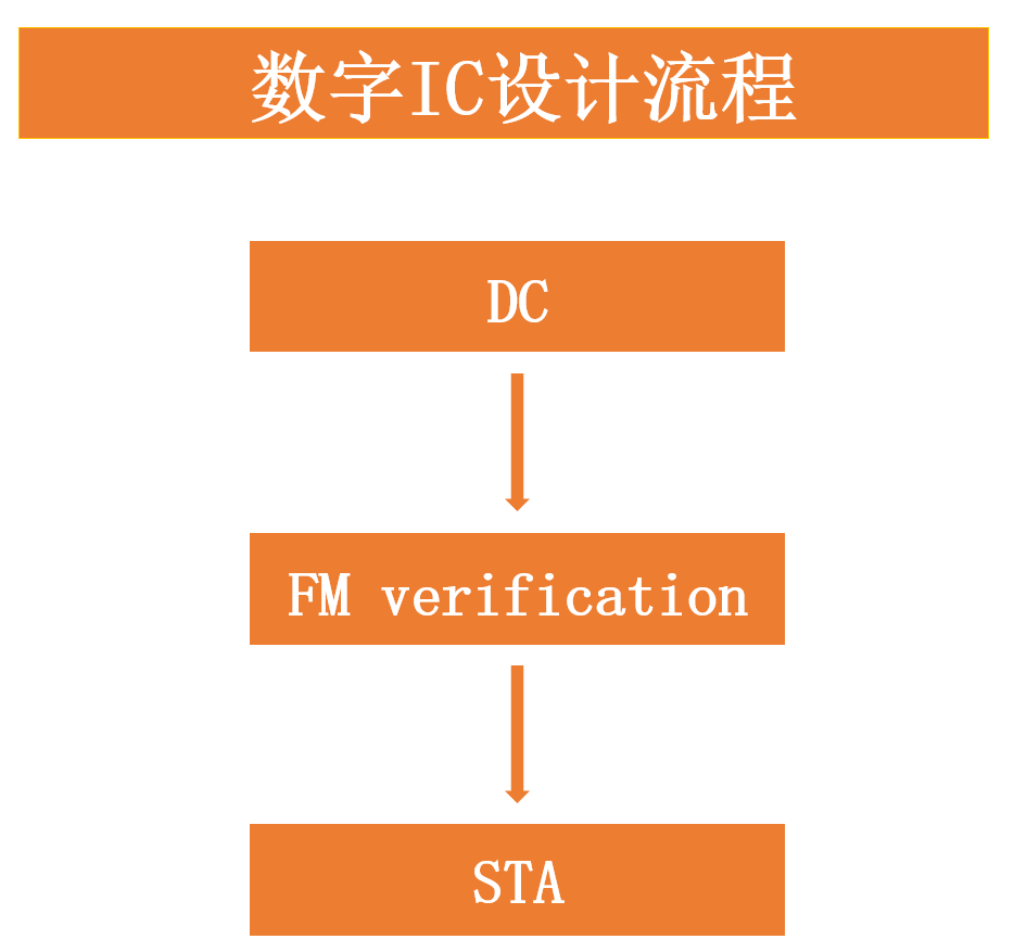
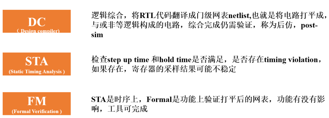
Back-end:
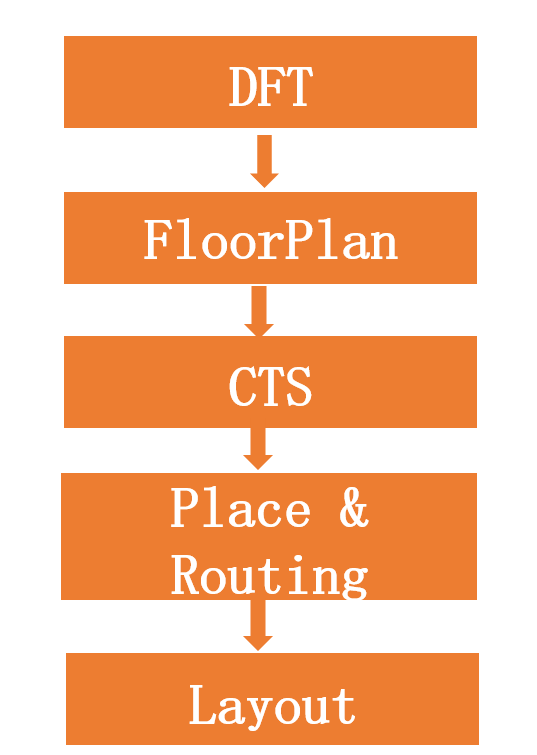
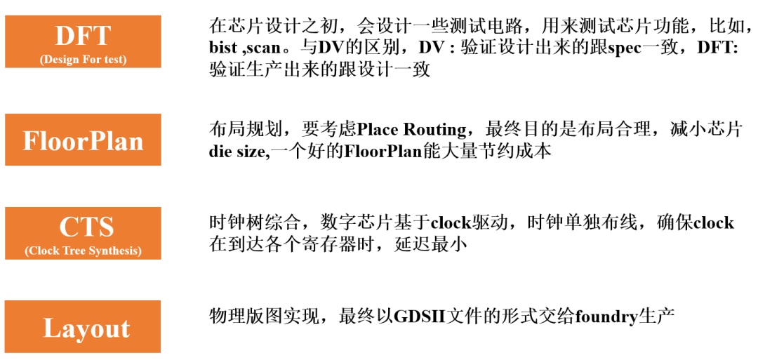
02 Digital IC Position Introduction
Engineer Overview: Each process generally has corresponding engineers
●Front-end: Chip Architecture Engineer
Chip Design Engineer
Chip Verification Engineer
●Mid-end and Back-end: Physical Design, DFT Engineer, Layout Engineer
Except for architecture and design, the rest can be outsourced, with back-end being the most outsourced; GUC and Global Foundry have professional back-end teams.
Positioning of Digital Verification Engineers:
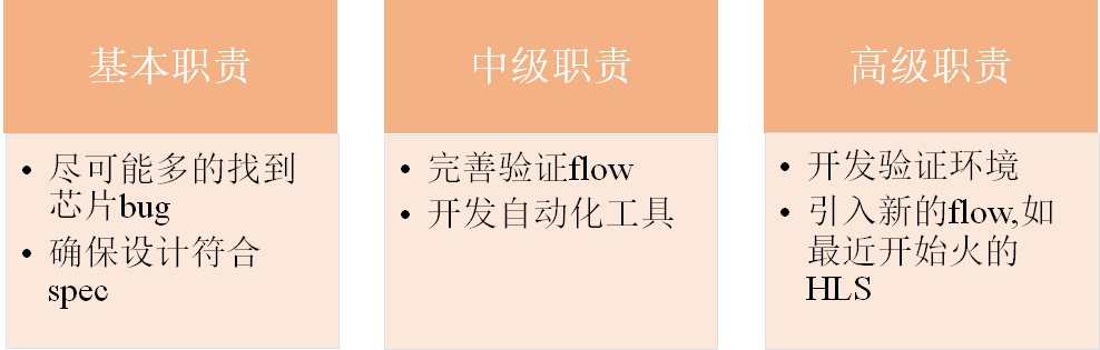
Personnel Distribution:Design: Verification is between 1:1 and 1:2
Verification workload occupies more than 60% of chip front-end workload, which is very important.
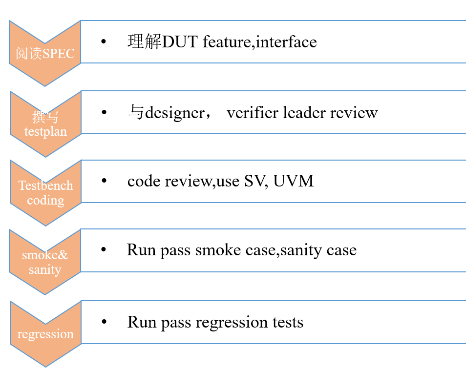
Digital Verification Work Content:
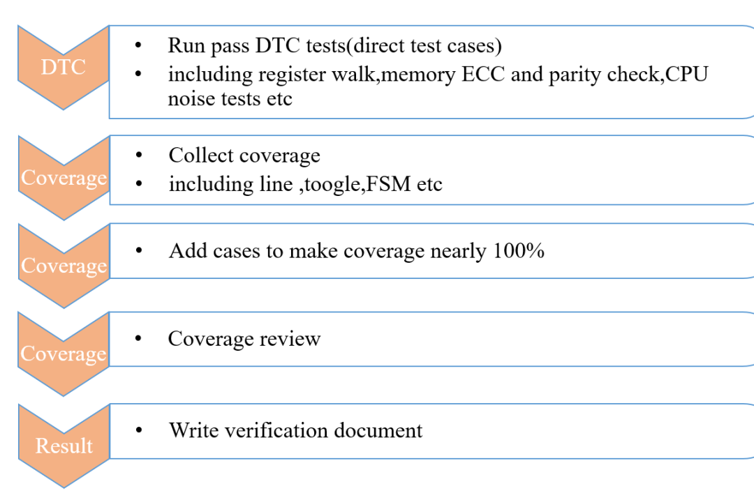
Digital Verification Development Direction:
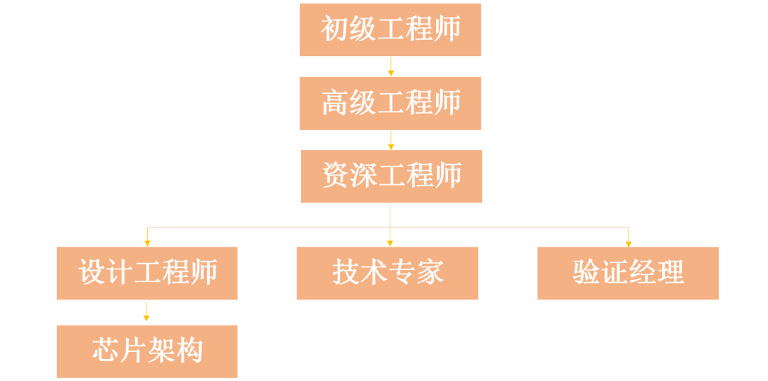
Knowledge to Learn for Digital Verification:
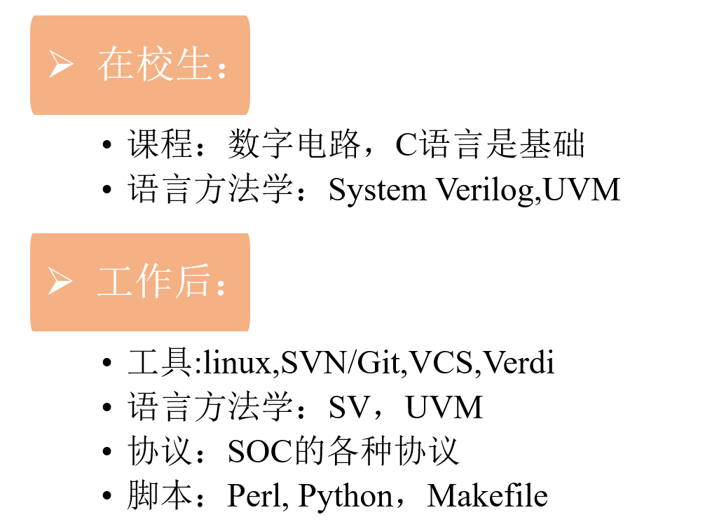
Market Demand for Digital Verification:
Due to the impact ofthe China-US trade war, chips have become a key bottleneck; in recent years, microelectronics has become one of the hot majors. At the same time, due to the popularity of AI and blockchain, a large amount of capital has flooded in, resulting in many start-up companies, such as Cambricon, Bitmain, Horizon Robotics, Deep Glint, etc., which were basically established around 2015. Meanwhile, some large companies are also increasing investment or forming their own chip teams, such as Alibaba’s Pingtouge, HiSilicon’s increasing number of self-developed chips, and Oppo’s newly formed chip team, etc.
Various AI chips have been launched, with processes getting lower and lower, the latest reaching 7nm, and the cost of a single tape-out can reach hundreds of millions, with ECO costing several million. As costs increase, fault tolerance decreases, as every ECO bug costs millions.
High costs raise the demand for high-quality chips, and design quality is determined by the verification quality of the DV team, thus digital verification has become a relatively scarce position in the market.
From my experience over the past few years, I have basically been undercut by new graduates every year.
The increase in market demand is reflected in two aspects:
a) More opportunities, with numerous opportunities from start-ups and large companies
b) Rising salaries, for both fresh graduates and experienced hires
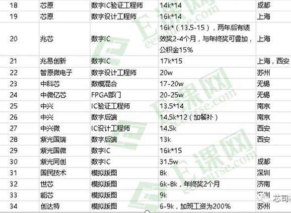
Salary and benefits for campus recruitment in 2020 for some companies:
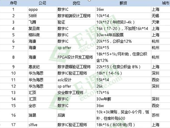
05
EDA Direction
01 EDA Laboratory Introduction
EDA Introduction: Electronic Design Automation (EDA) refers to the use of computer-aided design (CAD) software to complete the design process of ultra-large-scale integrated circuits (VLSI) chips, including functional design, synthesis, verification, and physical design (including layout, routing, layout design rule checking, etc.). Common software includes Virtuoso, ICC2, Calibre
CurrentTeachers: Zeng Xuan, Yang Fan, Yan Changhao, Tao Jun. Among them, Teacher Zeng Xuan is the core of the EDA laboratory. Current research directions include but are not limited to, automated design of analog circuits, Bayesian optimization. For specific research directions of each teacher, refer to the faculty directory of Fudan Microelectronics Institute.
02 Training Methods
PhD: For example, the five-year direct PhD program mainly involves research work in the first two years, accumulating professional knowledge, determining research directions and goals, and focusing on publishing papers in the last three years.
Academic Master’s: The first year mainly involves research work, and the second year focuses on publishing articles. After completing graduation requirements, students may need to assist teachers with some auxiliary research tasks.
Engineering Master’s: Because there are no specific academic requirements, and there is a hard requirement for internship experience, students are generally sent for internships. Partner internship units include Synopsys, Anlu Technology.
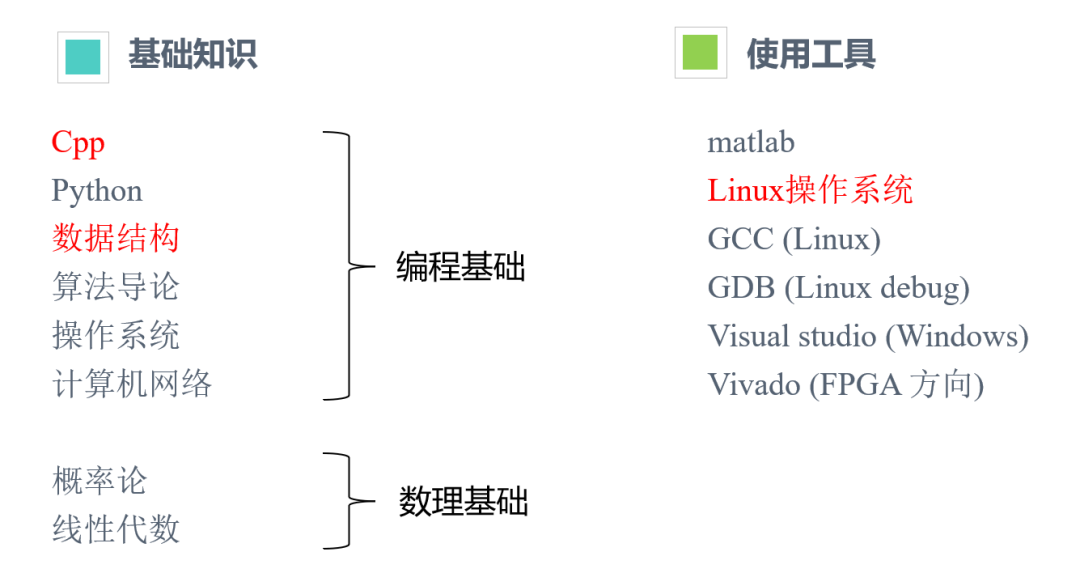
03 Professional Requirements
04 Employment Choices
The vast majority choose to go to internet companies, such as Alibaba, Tencent, Toutiao
A small number choose to go to specialized companies, such as Huawei, Cadence
A very small number choose completely unrelated industries, such as finance, teaching
05 Industry Status
Current Industry Giants:
Synopsys: DC, PT, ICC2, IP design
Cadence: Virtuoso, Innovus
Mentor: Calibre
Domestic EDA:
Huawei
Hongxin Micro-Nano
EDA Innovation Center
 END
END