Welcome FPGA engineers to join the official WeChat technical group.
Clickthe blue textto follow us at FPGA Home – the best and largest pure FPGA engineer community in China.

When designing chips, the first thing to focus on is the chip’s PPA (Performance, Power, Area). This article discusses the second P, Power consumption, and how to achieve low power design in RTL design, which is crucial for the endurance of mobile devices. Don’t let your chip increase power consumption unnecessarily.
Data Path Register Sampling
Data registers sample with vld and do not add reset logic, which saves wiring area for the reset circuit of the register. Moreover, the tool will automatically insert clock gating for the register, achieving a reduction in power consumption.As for registers without reset, some beginners may find this a bit refreshing. How can a register not be reset? Isn’t not resetting it just producing an x state, which would confuse the system? Yes, not resetting a register will produce an x state; however, we are discussing the data path here, while all signals in the control path must include reset logic. In the data path, as long as it is valid when you use it, it doesn’t matter if it is in an x state. The control path signals control the operation of the system, and if an x state occurs, it will definitely hang. The data path only needs to ensure that it is valid when vld is active, meaning that when I access this data, it is correct, regardless of whether it is in an x state or other invalid data.Of course, if the data is used for logic judgment for control, then this data must be reset.Code example: in sequential logic, you can omit else; the register maintains its default state, while in combinational logic, you must write else. vld is a pulse that pushes this data directly into the register for storage, and this register will hold this data until the next pulse arrives.
always @(posedge clk)begin if(data_vld) dout[63:0] <= din;end
Manually Insert Clock Gating
Manually inserting clock gating can automatically turn off the clock of some modules based on different control scenarios, leaving a control channel for software to shut down. This can effectively reduce dynamic power consumption.For example, when a computation circuit is configured to be fully on, it needs four identical computation modules to work simultaneously, while in the minimum case, only one module needs to work. In this case, based on different configurations, the clocks of the other three modules can be turned off to reduce dynamic power consumption.
Power Down the Entire Top Module
The entire secondary Top module can be powered down for sleep. After power down, all necessary data should be written to memory, and when the module is awakened and powered on again, the data should be rewritten back to the hardware. In ASIC, the RAM can generate whether it needs to power down to save data, and RAM that does not need to store data can also be powered down.If the number of data registers that need to be used and saved is small, you can extend interfaces from the module to the top layer, allowing software to read them, and when the module is awakened and powered on, the registers can be configured back to the module via software. This is low power mode.
Static Power Consumption and Dynamic Power Consumption
Static power consumption exists as long as the circuit is powered, and unless it is powered down for sleep, it cannot be avoided. Dynamic power consumption occurs whenever there is a high-low voltage transition. In RTL design, good coding style can also reduce dynamic power consumption. Arithmetic units like multipliers and adders can reduce dynamic power consumption by minimizing the switching of combinational logic.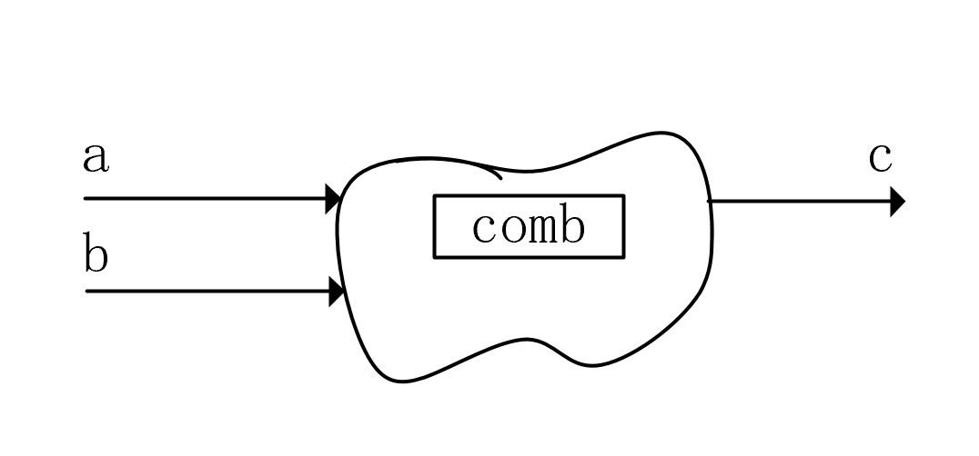 From input to output, if the values of combinational logic at a and b remain unchanged, there will be no voltage transitions, thus avoiding dynamic power consumption, only static power consumption exists. In design, consider the issue of invalid transitions in combinational logic; during certain periods, if this part of the data is invalid, you can use enable signals to select this logic to hold, achieving the effect of avoiding dynamic power consumption.
ScanOnce
FPGA Home

Welcome FPGA, embedded, signal processing engineers to follow our public account.
Follow meto join us!
Engineers!
The largest FPGA technical group community in the country.

Welcome everyone to join the largest and strongest FPGA WeChat technical group. This group has tens of thousands of engineers, a group of engineers who love technology, where FPGA engineers help each other and share knowledge, creating a strong technical atmosphere!Quickly invite your friends to join!

Just press with your finger to join the national FPGA technical group!

One of the best Xilinx and Altera chip suppliers in the country!
Platform self-operated, imported original quality guarantee!
Continuously supplying multiple military research institutes and listed companies!
The best FPGA chip prices and the best after-sales service!
With the industry’s top service reputation!
Backed by global top supplier quality standards!
Full range of XILINX orders or spot advantages!
XCVU9P-2FLGB2104I 200PCS
XCVU9P-2FLGA2104I 500PCS
XCVU13P-2FLGB2104I 300PCS
XC7K325T-2FFG900I 1500PCS
XC7K325T-2FFG676I 950PCS
XC7K160T-2FFG676I 850PCS
XC7VX690T-2FFG1927I Coming soon, please reserve!
XC7VX690T-2FFG1761I Coming soon, please reserve!
For more Xilinx model inquiries, please consult us! Thank you! Scan the QR code to join!
Official thanks to the FPGA technical group brands: Xilinx, Intel (Altera), Microsemi (Actel), Lattice, Vantis, Quicklogic, Lucent, etc., for their support of the technical group!