Welcome FPGA engineers to join the official WeChat technical group
Clickthe blue textto follow us at FPGA Home – the best and largest pure FPGA engineering community in China

LVDS
stands for Low-Voltage Differential Signaling. The selectIO of FPGA is very powerful, supporting various IO interface standards, with voltage and current configurable. Its interface rate can reach hundreds of M or even thousands of M. Using LVDS to receive data generated by high-speed ADC is very convenient. Resources like ISERDES, IDDR, IDELAY, OSERDES, and ODDR are abundant in FPGA’s IOB (each IO corresponds to one, which will be introduced later), so there is no worry about usage. Recently, I just used it in a project and would like to provide an idea; specific device usage can refer to the FPGA manual.
The AD chip used is ADI’s AD9653, a 125M 16-bit high-precision high-speed ADC, with a sampling rate of 80M. The SPI configuration will be discussed in a separate article; there is a major pitfall in the SPI configuration. Initially, I thought it was set correctly, but later I discovered problems and spent three days to locate the issue, which is the charm (and the pain) of hardware. Here, I will mainly introduce the receiving part of the FPGA.
The timing diagram for receiving ADC data,
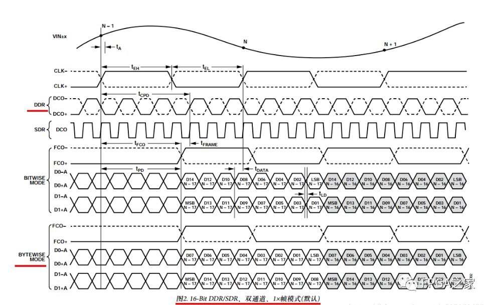
There are a few points to note:
0, It can be seen that there are three types of signals: data sampling clock DCLK, frame synchronization signal FCLK, and input data DATA
1, The input data sampling clock is by default aligned to the midpoint of the input data, but the frame clock is aligned to the edge of the data byte.
2, Use Iserdes to receive data, and Idelay to adjust clock delay.
1, The processing of the data sampling clock is as follows
By controlling the delay, make CLK align with the BitClk passing through IBUFDS, thus eliminating the delays of IBUFIO, BUFR, and net. This way, all input signals only go through one IBUFDS, with equal delays. The control of Idelay can be manually adjusted or done using an automatic algorithm. (Refer to xapp524)
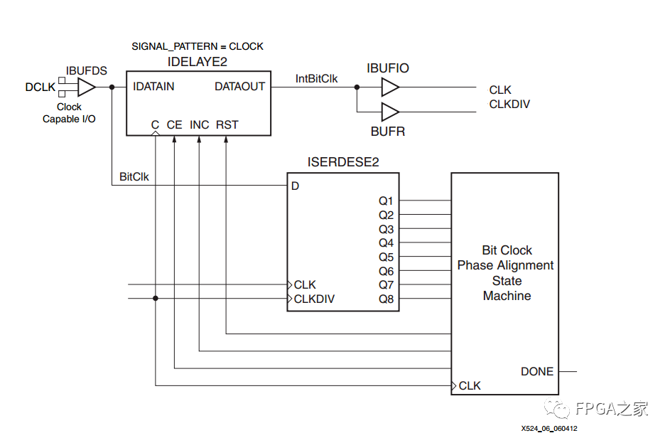
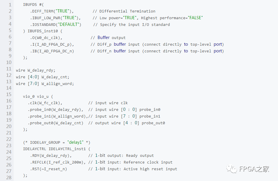
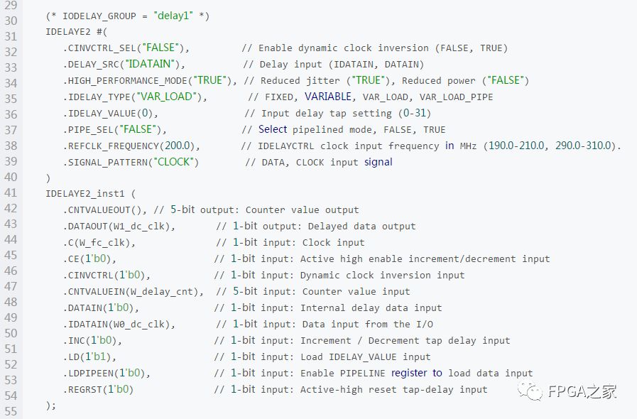
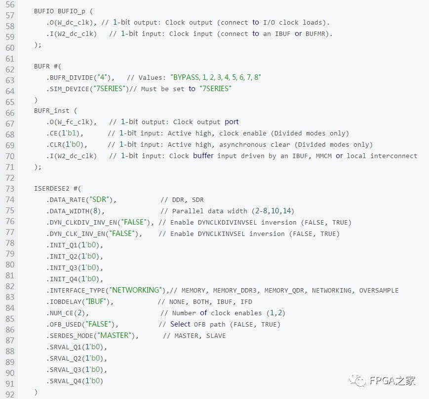
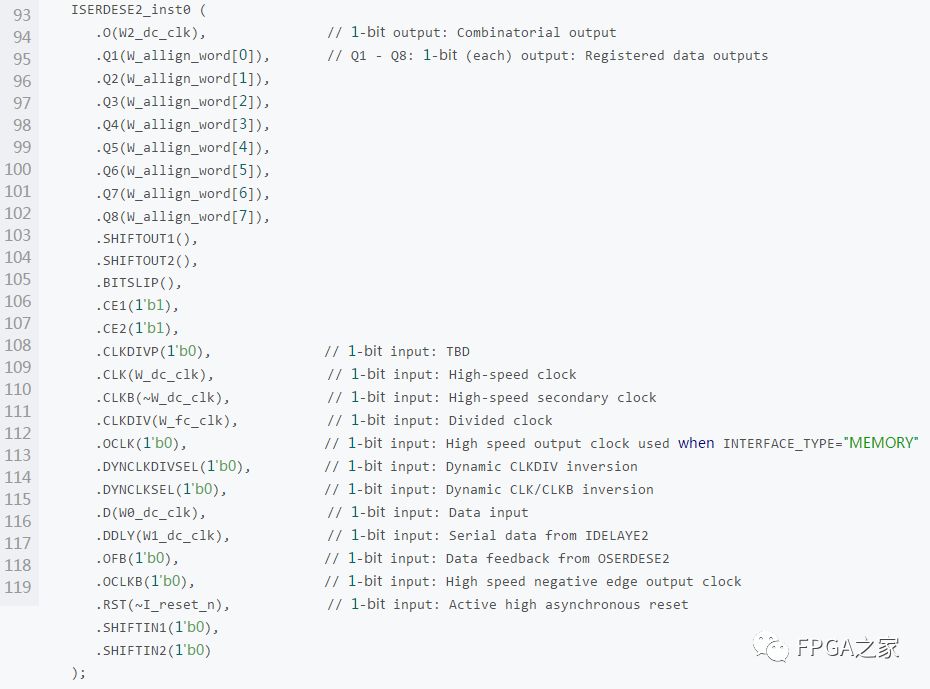
1.1 Manual Adjustment of Alignment
First, let’s look at the manual adjustment algorithm. Using Vivado’s VIO, it is very convenient to input and output, and you can manually modify and observe phenomena online, which also provides some inspiration for the subsequent automatic training algorithm. When R_delay_cnt=0 by default, the input sine wave looks very messy
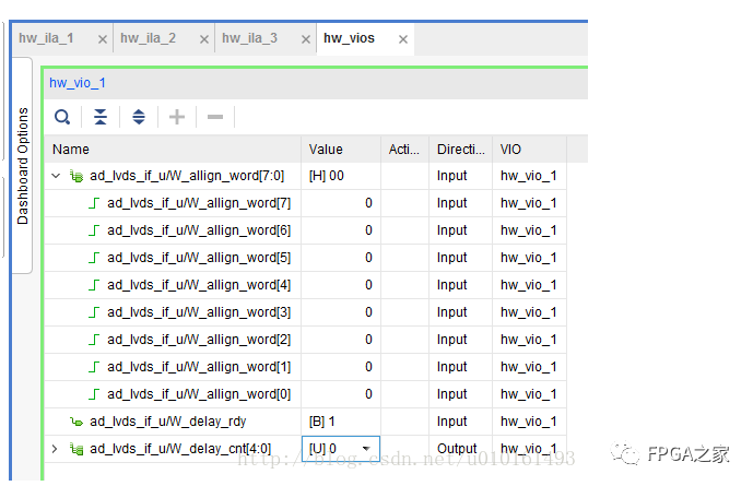
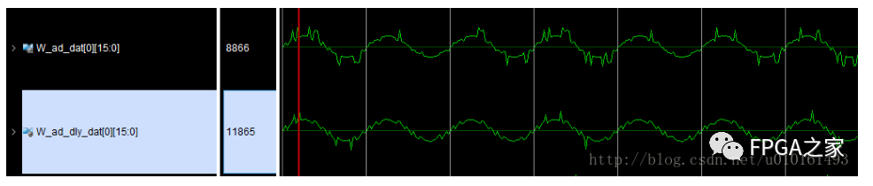
Slowly increase R_delay_cnt, when R_delay_cnt=12, a stable sine wave begins to appear. Experiments found that R_delay_cnt=14, 15, 16 happen to catch the edges of the clock, which aligns with the original input clock. It can be seen that catching the edge causes allign_word to keep changing, with some being 0 and others being 1. Until R_delay_cnt=18, the sine wave remains stable. The effective window can be accurately calculated, with a 200M Idelay reference clock, 78ps/tap. 7tap*78ps=546ps. This shows that the effective window of the data is very small, after all, it is 320M DDR, and half a cycle is only 1.56ns.
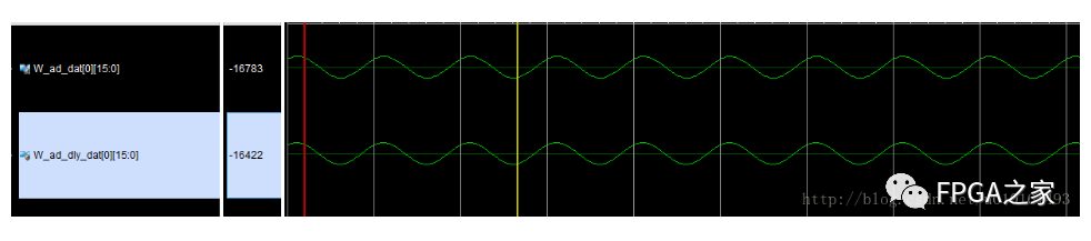
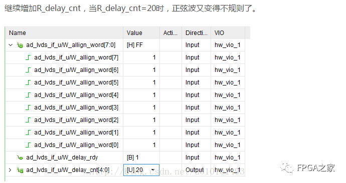
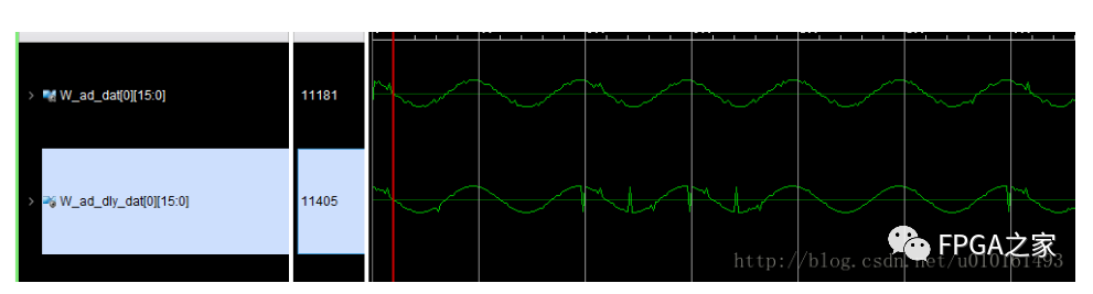
Finally, set R_delay_cnt=15, which can be hardcoded in the code.
1.2 Automatic Training Algorithm
Since there is a manual adjustment algorithm, why still use an automatic training alignment algorithm? During high and low temperature testing, the delay of the device will change due to temperature effects, especially when the clock frequency is very high and the effective data window is very small. At this time, it is necessary to dynamically change the value of R_delay_cnt to adapt to the changes in delay, increasing robustness.
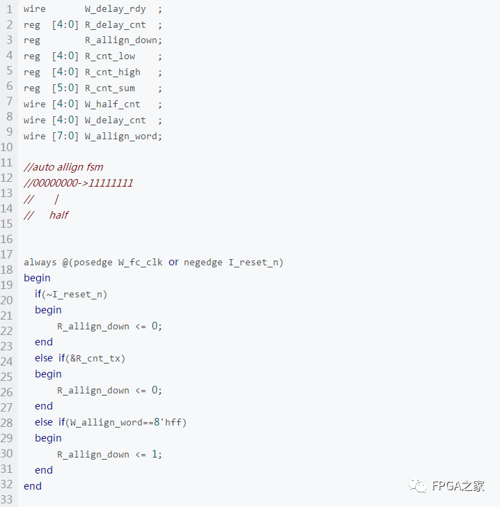
With the manual adjustment algorithm above, the idea for automatic training is also very simple. After power-on reset, R_delay_cnt keeps incrementing, recording the last all-zero and the first all-one values, taking the midpoint. Only one case is considered here; there could also be a case from all-one to all-zero. The code is as follows
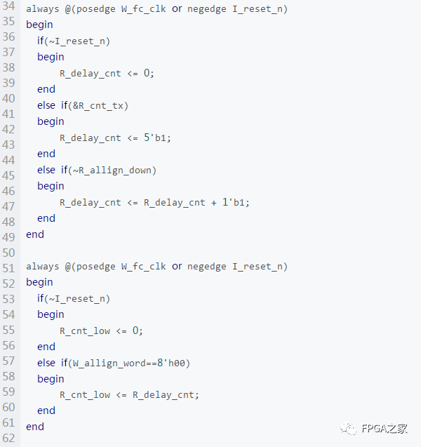
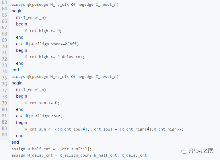
2, Processing of Frame Synchronization Signal and Data
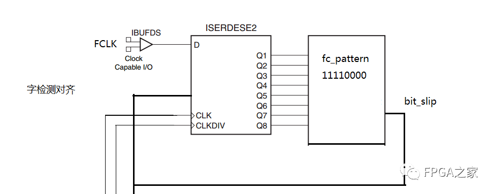
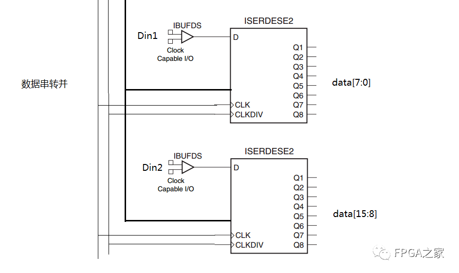
Using the data sampling clock generated above to sample FCLK and DATA simultaneously, using Iserdes can perform 1:8 serial to parallel conversion. However, we do not know where the byte boundaries are, so we need to use a bit_slip to shift the result of serial to parallel conversion, while detecting the output of FCLK conversion. When the output is 8’b11110000, stop shifting.
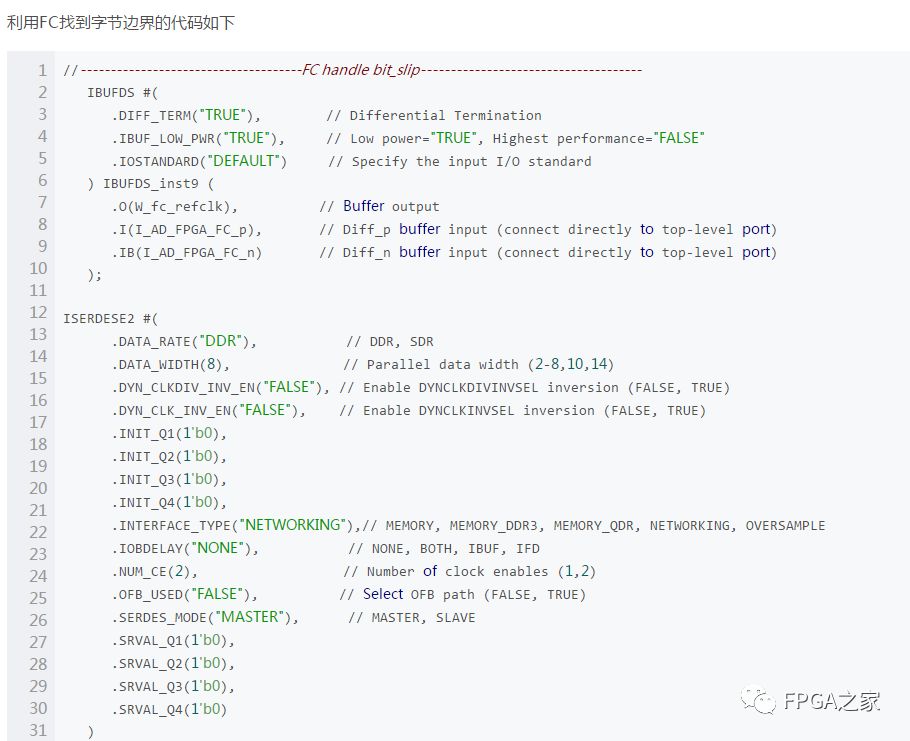
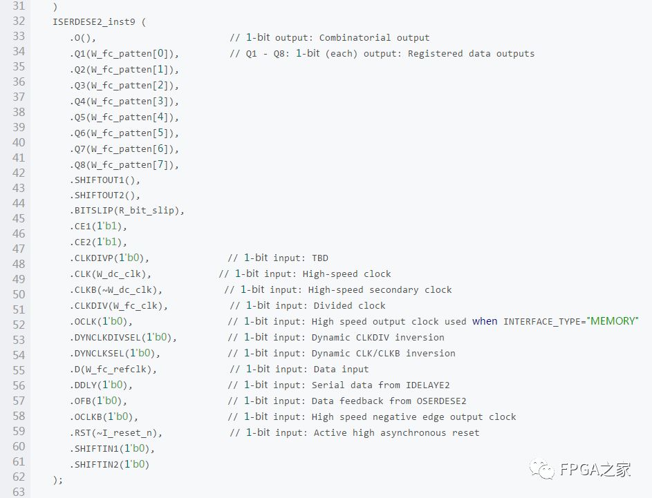
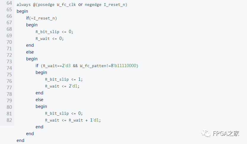
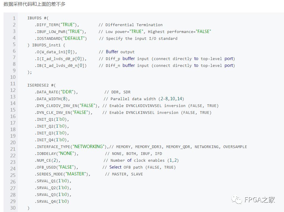
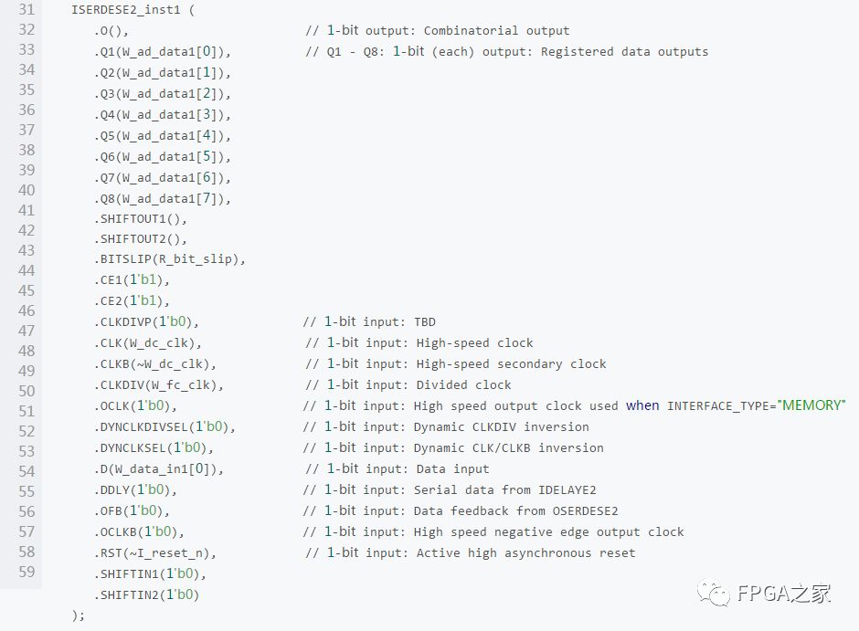
When the data rate is not very high for IDDR data, use DDR instead of Iserdes for reception. IDDR and Iserdes use the same resources (to be verified)
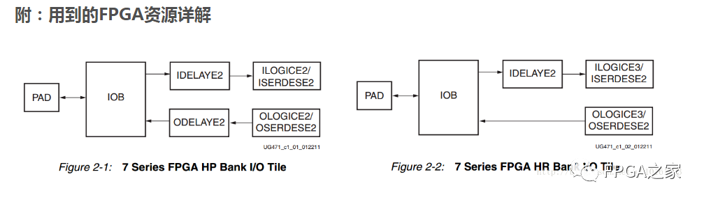
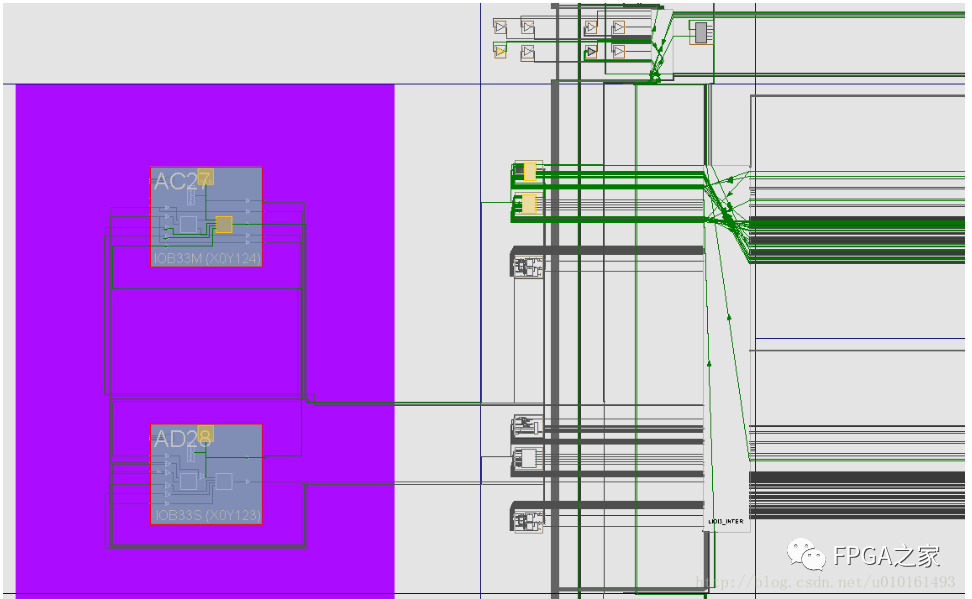
The real device of HR Bank is as follows, a pair of IOBs, can be used separately or differentially. The subsequent resources from top to bottom are ISERDES (ILOGIC), IDELAY, OLOGIC (OSERDES), ILOGIC, IDELAY, OLOGIC. (ILOGIC can act as IDDR, OLOGIC can act as ODDR). The upper left corner is a clock region (e.g., X0Y2) with four BUFIO and BUGR (local clock drive, local clock frequency division, both with equal delays) distributed in the middle. The following is an IDELAYCTRL.
The following will detail: IDEALY, must go through ISERDES after IDELAY, can be passed directly. ISERDES, ISERDES and ILOGIC use the same resources and can be interchanged. ILOGIC,
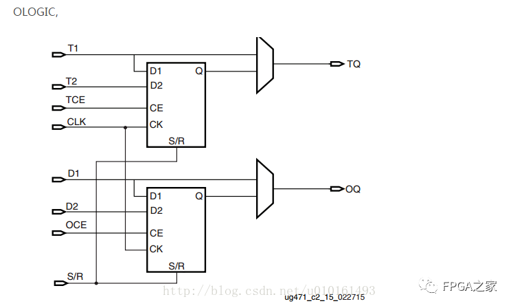
OSERDES, and OLOGIC use the same resources and can be interchanged.
Function Description
• Edge triggered D type flip-flop (FF)
• DDR mode (SAME_EDGE or OPPOSITE_EDGE)
• Level sensitive latch (Latch)
• Asynchronous/combinatorial (pass-through)

Welcome FPGA engineers and embedded engineers to follow the public account

The largest FPGA WeChat technical group in the country
Welcome everyone to join the national FPGA WeChat technical group, which has tens of thousands of engineers, a group of engineers who love technology. Here, FPGA engineers help each other, share knowledge, and the technical atmosphere is strong!Hurry up and invite your friends to join!!

Press and hold to join the FPGA national technical group
FPGA Home Component City
Advantageous component services, please scan the code to contact the group owner: Jin Juan Email: [email protected] Welcome recommendations to procurement
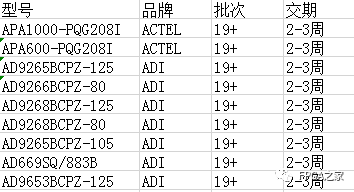
ACTEL, AD part of advantageous orders (operating the entire series):
XILINX, ALTERA advantageous stock or orders (operating the entire series):
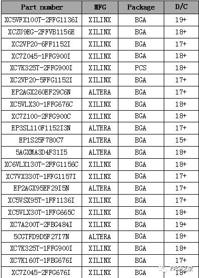
(The above devices are part of the models, for more models please consult group owner Jin Juan)
Service Philosophy: FPGA Home Component City aims to facilitate engineers in quickly and conveniently purchasing components. After years of dedicated service, our customer service is spread across large publicly listed companies, military research units, and small and medium enterprises. Our biggest advantage is emphasizing the service-first concept, and achieving fast delivery and favorable prices!
Direct brands: Xilinx ALTERA ADI TI NXP ST E2V, Micron and other hundreds of component brands, especially good at dealing with components under US restrictions on China,engineers are welcome to recommend us to procurement or consult us directly!We will continue to provide the best service in the industry!

Official thanks to brands in the FPGA technical group: Xilinx, Intel (Altera), Microsemi (Actel), Lattice, Vantis, Quicklogic, Lucent, etc.