Win a Backpack!
How Hard Is It?
Give It a Try!
→_→

Each transceiver has an independent transmitter, which consists of PMA (Physical Media Attachment) and PCS (Physical Coding Sublayer). The PMA sublayer includes circuits for high-speed serialization/deserialization (Serdes), pre/post-emphasis, receive equalization, clock generation, and clock recovery. The PCS sublayer includes circuits for 8B/10B encoding/decoding, buffers, channel bonding, and clock correction. For the GTX transmitter, the structure is shown in Figure 1.
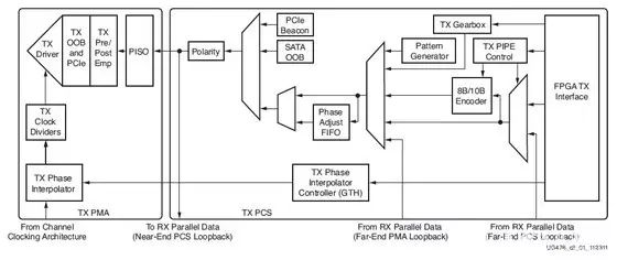
Figure 1
The internal parallel data of the FPGA enters the TX transmitter through the FPGA TX Interface, then processed by various functional circuits in the PCS and PMA sublayers, and finally output as high-speed serial data from the TX driver. Below, we will introduce each functional circuit.
FPGA TX Interface (TX User Interface): The TX Interface is the interface for user data sent to the GTX. The signals of this interface are shown in Table 1.
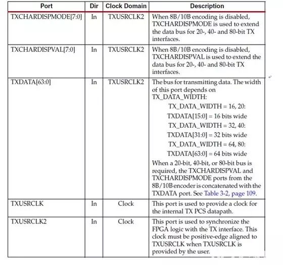
Table 1
The data transmission interface is TXDATA, the sampling clock is TXUSRCLK2, which samples TXDATA on the rising edge of TXUSRCLK2. The rate of TXUSRCLK2 is determined by the line rate, TX Interface width, and whether 8B/10B is enabled (TXUSRCLK2 frequency = line rate / TX_DATA_WIDTH; for example, if the line rate is 10Gb/s, and TX_DATA_WIDTH equals 80, then TXUSRCLK2 frequency is 125MHz).
TXDATA width can be configured to 16/20/32/40/64/80 bits. The configuration can be done through the attributes TX_DATA_WIDTH, TX_INT_DATAWIDTH, and TX8B10BEN, as shown in Table 2.
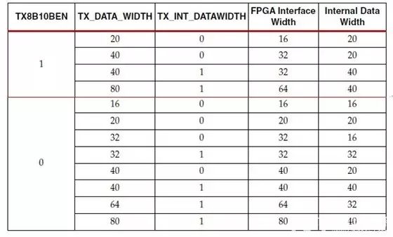
Table 2
The GTX TX Interface is divided into internal data width and FPGA interface width. The internal data belongs to the TXUSRCLK clock domain, while the FPGA interface data belongs to the TXUSRCLK2 clock domain. The internal data width supports 2byte/4byte, while the FPGA interface data width supports 2byte/4byte/8byte. Therefore, it determines that TXUSRCLK and TXUSRCLK2 have a certain clock multiplication relationship, as shown in Table 3. The TX_INT_DATAWIDTH attribute set to “0” indicates that the internal data width is 2byte, while setting it to “1” indicates an internal data width of 4byte (this should be set to “1” when the line rate exceeds 6.6Gb/s).
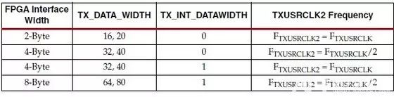
Table 3
TXUSRLK and TXUSRCLK2 clocks are related. The following two criteria should be followed for these two clocks:
-
1. TXUSRCLK and TXUSRCLK2 must be aligned on the rising edge, with minimal deviation. Therefore, BUFGs or BUFRs should be used to drive these two clocks (since there is no phase correction circuit or FIFO between the TX Interface and the PCS sublayer, strict alignment is needed, as per my understanding).
-
2. Even if TXUSRCLK, TXUSRCLK2, and the reference clock of GTX operate at different clock frequencies, all three must use a common source clock.
Clock Structure of the Transmitter: To better understand how the GTX transmitter works, it is necessary to understand the clock structure of the transmitter. Figure 2 is the clock structure diagram of the transmitter.
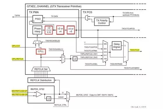
Figure 2
The content in the red box and yellow background is what we need to focus on. The MGTREFCLK in the figure is the reference clock of GTX mentioned in the previous article, which enters the GTX after passing through an IBUFDS_GTE2 source. It is used to drive CPLL or QPLL. For the TX PMA, the main function is to achieve serialization/deserialization. The clock for serialization/deserialization can be provided by CPLL or QPLL, selected by TXSYSCLKSEL. The three red box parts in the TX PMA sublayer are serial and parallel clock dividers, which are used to generate the driving clock for parallel data. The D divider is mainly used to divide the PLL output to support lower line rates.
÷2/÷4 is determined by TX_INT_DATAWIDTH. If TX_INT_DATAWIDTH is “0”, then ÷2 is selected; otherwise, ÷4 is selected.
For ÷4/÷5, it is determined by TX_DATA_WIDTH. If the width is 16/32/64, then ÷4 is selected; if the width is 20/40/80, then ÷5 is selected.
As for who drives TXUSRCLK and TXUSRCLK2, the official recommendation is to use TXOUTCLK as the driver, which simplifies the design while stabilizing it. How to use TXOUTCLK to drive TXUSRCLK and TXUSRCLK2? According to the frequency relationship of TXUSRCLK and TXUSRCLK2, taking one Lane as an example, Figure 3 shows the driving method where TXUSRCLK=TXUSRCLK2, and Figure 4 shows the driving method where TXUSRCLK = 2*TXUSRCLK2.
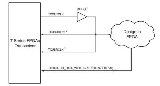
Figure 3
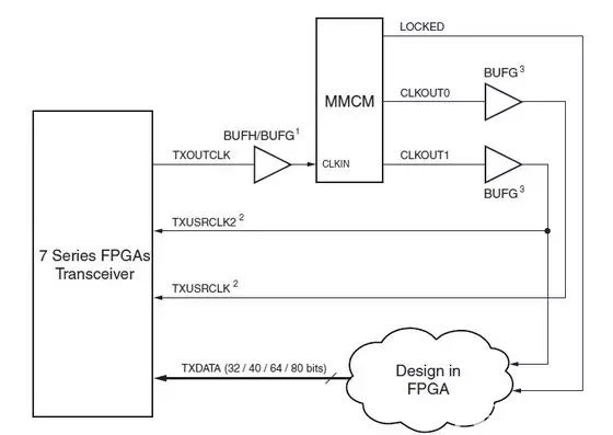
Figure 4
In Figure 4, the value of CLKOUT0 is twice that of CLKOUT1.
TX 8B/10B Encoder: The high-speed transceiver’s transmitter generally includes an 8B/10B encoder. The purpose is to ensure that the data has enough transitions to provide for clock recovery circuits. The encoder also provides a method for aligning data to words while maintaining good DC balance on the line. In GTX applications, if D codes are sent, TXCHARISK should be pulled low; if K codes are sent, the corresponding TXCHARISK should be pulled high.
TX Buffer: To understand the role of the transmitted TX Buffer, it is first necessary to clarify the clock domain of the TX transmitter. The clock domain of the TX transmitter is shown in Figure 5.
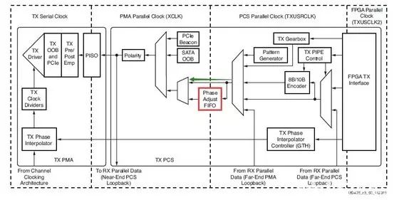
Figure 5
The red box in Figure 5 is the TX Buffer. We all know that FIFO has the function of isolating clock domains, and here is no exception. From the diagram, we can see that the TX Buffer connects two different clock domains, XCLK and TXUSRCLK. The PCS sublayer in the transmitter contains two clock domains, XCLK (PMA parallel clock domain) and TXUSRCLK clock domain. To ensure stable data transmission, XCLK and TXUSRCLK must match in rate and have phase differences eliminated. The TX Buffer is mainly used to match the rate of the two clock domains and eliminate the phase difference between them.
TX Buffer can also be bypassed. The TX transmitter provides a phase alignment circuit that can solve the phase difference between XCLK and TXUSRCLK clock domains. However, TX_XCLK_SEL must be set to “TXUSR” to keep the XCLK clock domain and TXUSRCLK in sync.
TX Pattern Generator: GTX has a pseudo-random number sequence generation circuit. The pseudo-random number sequence appears random but is actually a periodic binary sequence with good randomness and a correlation function close to white noise. Therefore, the pseudo-random number sequence can be used for bit error rate measurement, delay measurement, noise generation, communication encryption, and spread spectrum communication, etc. In GTX, it can be used to test the bit error rate of high-speed serial channel transmission. Figure 6 shows the PRBS generation circuit of GTX.
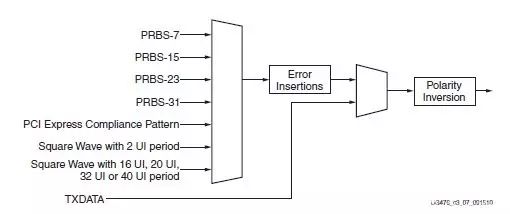
Figure 6
The PRBS generation circuit can be enabled or bypassed. If bypassed, TXDATA will be transmitted to the PMA of the transmitter. Generally, the PRBS mode test model is as shown in Figure 7.
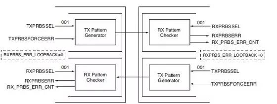
Figure 7
TX Polarity Control: The TX transmitter supports polarity control of the transmitted data. The encoded data output from the PCS sublayer undergoes polarity inversion before entering the PISO serialization. This function is mainly used to compensate for design errors in the PCB. If the PCB is designed incorrectly with TXP and TXN crossed, the signal polarity can be inverted by setting TXPOLARITY to “1”.