Welcome FPGA engineers to join the official WeChat technical group
Clickthe blue textto follow us at FPGA Home – the largest and best FPGA pure engineer community in China

Introduction: In this article, we introduce the global clock resources. The global clock is a dedicated interconnect network specifically designed to reach all clock inputs to various resources in the FPGA. These networks are designed to have low skew and low duty cycle distortion, low power consumption, and improved jitter tolerance. They are also designed to support very high-frequency signals. Understanding the signal paths of the global clock can extend the understanding of various global clock resources. The global clock resources and networks consist of the following paths and components:
-
Clock trees and networks: GCLK
-
Clock regions
- Global clock buffers
1. Clock Trees and Networks: GCLK
The clock trees of the 7 series FPGA are designed for low skew and low power operation, with any unused branches of the clock being disconnected. The clock trees can also be used to drive logic resources, such as reset or clock enable, primarily used for high fan-out/load networks. In the architecture of the 7 series FPGA, access to the pins of the global clock lines is not limited to the clock pins of logic resources. The global clock lines can drive pins in the CLB other than the CLK pins (e.g., control pins SR and CE). Applications requiring very fast signal connections and large load/fan-out can benefit from this architecture.
2. Clock Domains
The 7 series devices improve clock distribution by using clock regions. Each clock region can have up to 12 global clock domains. These 12 global clocks can be driven by any combination of 32 global clock buffers in a single device or SLR. The size of the clock regions is fixed at 50 CLBs high (50 IOBs), spanning either the left or right side of the die. In the 7 series devices, the clock backbone divides the device into left and right sides. By fixing the size of the clock regions, larger 7 series devices can have more clock regions. The 7 series FPGA provides 1 to 24 clock regions.
3. Global Clock Buffers
There are up to 32 global clock buffers in the 7 series devices. CCIO inputs can be directly connected to any global clock buffer in the same half of the device. Each differential clock pin pair can be connected to differential clocks or single-ended clocks on the PCB. When used as a differential clock input, it connects directly to the P side of the differential input pin pair. When used as a single-ended clock input, it must use the P side of the pin pair, as direct connections only exist on that pin. For pin naming conventions, refer to UG475: 7 Series FPGA Packaging and Pinout Specifications. If a single-ended clock is connected to the P side of a differential pin pair, the N side cannot be used as another single-ended clock pin. However, it can be used as a user I/O. The CMT in the upper half of the device can only drive the BUFG in the upper half of the device, and the CMT in the lower half can only drive the BUFG in the lower half. Similarly, only BUFGs in the same half of the device can be used as feedback to the CMT in the same half of the device. When the CMT column extends to an area containing both GT and I/O columns, the Gigabit transceivers (GTs) can only be directly connected to MMCMs/PLLs. The Virtex-7T and Virtex-7XT devices have these complete columns. GTs and CMTs in Spartan-7, Artix-7, Kintex-7, and Zynq-7000 devices can only be connected using BUFHs (preferred) or BUFGs. Global clock buffers allow various clock/signal sources to access the global clock tree and network. Possible sources to the global clock buffers include:
-
Clock inputs
-
Clock management blocks (CMT) driving BUFG in the same half of the device
-
Outputs from neighboring global clock buffers (BUFGs)
-
Generic interconnect
-
Regional clock buffers (BUFRs)
- Transceivers
The 7 series FPGA clock inputs can indirectly drive global clock buffers through vertical clock networks in the clock backbone column. The 32 BUFGs are divided into two groups, each containing 16 BUFGs, located at the top and bottom of the device. Any resources directly connected to the BUFGs (e.g., GTX transceivers) have a top/bottom constraint. For example, each MMCM at the top can only drive the 16 BUFGs at the top of the device. Similarly, the MMCMs at the bottom drive the 16 BUFGs at the bottom.
All global clock buffers can drive all clock regions in the 7 series devices. However, only 12 different clocks can be driven within a single clock region. The clock buffers are designed with a synchronous or asynchronous glitch-free 2:1 multiplexer with two clock inputs. The BUFG cascade has a dedicated path (routing resources) that allows selection of more than two clock inputs. The clock control pins of the 7 series FPGA provide extensive functionality and powerful input switching. In the clock structure of the 7 series FPGA, the BUFGCTRL multiplexer and all derivatives can be cascaded within adjacent clock buffers of the 16 BUFGMUX groups in the upper and lower halves of the device, effectively creating a 16 BUFGMUX (BUFGCTRL multiplexer) ring in the upper half and another in the lower half. Figure 1 shows a simplified diagram of the cascaded BUFGs.
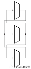
Figure 1, Cascaded BUFGsThe following subsections detail various configurations, primitives, and usage models of the 7 series FPGA clock buffers.
3.1 Global Clock Buffer Primitives
The primitives in Table 1 are different configurations of the global clock buffers. The ISE® or Vivado® design tools manage the configurations of all these primitives, and the constraint guidelines describe the LOC constraints.
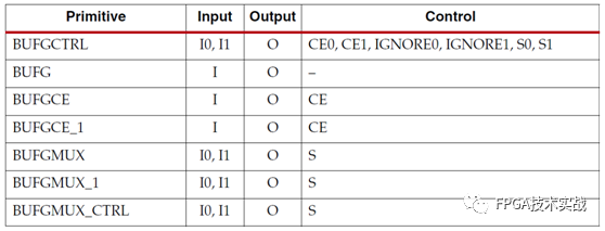
Table 1, Global Clock Buffer Primitives
BUFGCTRL
The block diagram of the BUFGCTRL primitive is shown in Figure 2, which can implement two-way asynchronous clock switching. All other global buffer statements can be obtained from some configuration of BUFGCTRL. BUFGCTRL has four selection ports: S0, S1, CE0, and CE1, plus two auxiliary control lines, IGNORE0 and IGNORE1. These six signals are used to control inputs I0 and I1.
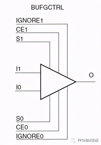
Figure 2, BUFGCTRL PrimitiveBUFGCTRL is used to switch between two clock inputs without generating glitches. When the currently selected clock changes from high to low after S0 and S1 change, the output remains low until another (to be selected) clock changes from high to low. Then the new clock begins to drive the output, and the default configuration of BUFGCTRL is falling edge sensitive, holding low before the input switches. BUFGCTRL can also be rising edge sensitive and use the INIT_OUT attribute to hold high before the input switches. In some applications, the above conditions are undesirable. Asserting the IGNORE pins bypasses BUFGCTRL to detect conditions when switching between two clock inputs. In other words, asserting IGNORE causes the MUX to switch inputs when the selection pins change. When the selection pins change, IGNORE0 switches the output immediately from I0 input, while IGNORE1 switches the output immediately from I1 input when the selection pins change. Selecting an input clock requires a “selection” pair (S0 and CE0, or S1 and CE1) to be asserted high. If S or CE is not asserted high, the required input will not be activated. During normal operation, the S and CE pairs (all four selection lines) should not be asserted high simultaneously. Typically, only one pin in the “selection” pair is used as a selection line, while the other pin is tied high. The truth table is shown in Table 2.
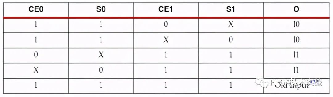
Table 2, Clock Resource Truth TableAlthough both S and CE are used to select the desired output, it is recommended to use only S for glitch-free switching. This is because the change in clock selection when using CE may be faster than when using S. The setup/hold time of the CE pins may cause glitches in the clock output. On the other hand, using the S pin allows switching between two clock inputs without considering setup/hold times. Therefore, using S to switch clocks does not cause glitches. See BUFGMUX_ CTRL. The timing diagram in Figure 3 illustrates various clock switching conditions using the BUFGCTRL primitive.
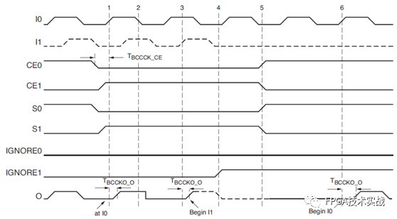
Figure 3, Timing Diagram of BUFGCTRL PrimitiveBefore event 1, output O uses input I0; other functions of BUFGCTRL include:
-
Pre-selection of inputs I0 and I1 is performed after configuration but before the device operates.
-
The initial output after configuration can be selected to be high or low.
- Clock selection using only CE0 and CE1 (with S0 and S1 tied high) can change clock selection without waiting for the previously selected clock to transition from high to low.
Table 3 summarizes the properties of the BUFGCTRL primitive.
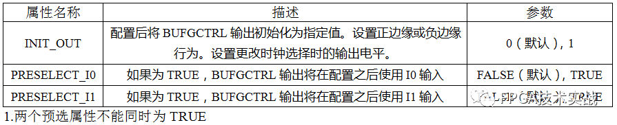
Table 3 BUFGCTRL Properties
BUFG
BUFG is a clock buffer with one clock input and one clock output. This primitive is based on BUFGCTRL, with some pins connected to logic high or low. Figure 4 illustrates the relationship between BUFG and BUFGCTRL. Constraints can be manually placed.
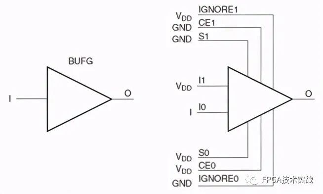
Figure 4, BUFG and BUFGCTRLThe timing diagram for BUFG is shown in Figure 5. The diagram shows the clock delay introduced by BUFG.

Figure 5, BUFG Timing Diagram
BUFGCE and BUFGCE_1
Unlike BUFG, BUFGCE is a clock buffer with one clock input, one clock output, and one clock enable line. This primitive is based on BUFGCTRL, with some pins connected to logic high or low. Figure 6 illustrates the relationship between BUFGCE and BUFGCTRL. LOC constraints can be used to manually place BUFGCE and BUFGCE_1 locations.
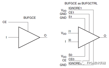
Figure 6, BUFGCE and BUFGCTRLThe switching conditions for BUFGCE are similar to those of BUFGCTRL. If the CE input is low before entering the rising clock edge, subsequent clock pulses will not pass through the clock buffer, and the output remains low. During the clock high pulse, any level change of CE has no effect before the clock transitions to low. When the clock is disabled, the output remains low. However, when the clock is disabled, it will complete the clock high pulse. Since the clock enable line uses the CE pin of BUFGCTRL, the selection signal must meet setup time requirements. Violating this setup time may cause glitches. Figure 7 illustrates the timing diagram for BUFGCE.
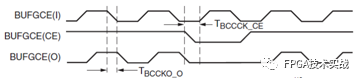
Figure 7, Timing Diagram of BUFGCEBUFGCE_1 is similar to BUFGCE, except its switching conditions differ. If the CE input is low before entering the falling clock edge, subsequent clock pulses do not pass through the clock buffer, and the output remains high. During the clock low pulse, any level change of CE has no effect before the clock transitions to high. When the clock is disabled, the output remains high. However, when the clock is disabled, it will complete the clock low pulse.
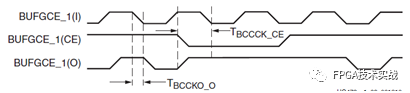
Figure 8, Timing Diagram of BUFGCE_1
BUFGMUX and BUFGMUX_1
BUFGMUX is a clock buffer with two clock inputs, one clock output, and one selection line. This primitive is based on BUFGCTRL, with some pins connected to logic high or low. Figure 9 illustrates the relationship between BUFGMUX and BUFGCTRL. LOC constraints can be used to manually place BUFGMUX and BUFGCTRL locations.
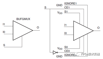
Figure 9, BUFGMUX and BUFGCTRLSince BUFGMUX uses the CE pin as a selection pin, the setup time requirements must be met when using the selection pin. Violating this setup time may cause glitches. The switching conditions of BUFGMUX are the same as those of the CE pin of BUFGCTRL. Figure 10 shows the timing diagram of BUFGMUX.
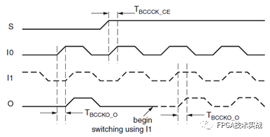
Figure 10, Timing Diagram of BUFGMUX
BUFGMUX_1 is rising edge sensitive, holding high before the input switches. Figure 11 shows the timing diagram for BUFGMUX_1. LOC constraints can be used to manually place BUFGMUX and BUFGMUX_1 locations.
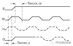
Figure 11, Timing Diagram of BUFGMUX_1

Welcome FPGA, embedded, signal processing and other engineers to follow the public account

Welcome to join the largest FPGA WeChat technical group in the country
Welcome everyone to join the national FPGA WeChat technical group, this group has tens of thousands of engineers, a group of technology-loving engineers, where FPGA engineers help each other and share, creating a strong technical atmosphere!Hurry up and invite your friends to join!!

Press and hold to join the national FPGA technical group
FPGA Home Component City
Advantageous component services, please scan the code to contact the group owner: Jin Juan Email: [email protected] Welcome to recommend to procurement
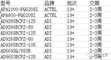
ACTEL, AD some advantageous ordering (operating the full range):
XILINX, ALTERA advantageous stock or ordering (operating the full range):
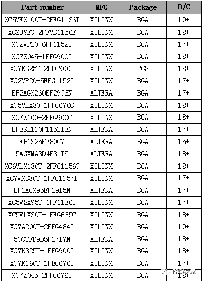
(The above devices are part of the model, for more models please consult the group owner Jin Juan)
Service concept: FPGA Home component self-operated city aims to facilitate engineers to quickly and conveniently purchase component services. After years of dedicated service, our customer service covers large listed companies, military research units, and small and medium-sized enterprises. The greatest advantage is emphasizing the principle of service first, and achieving fast delivery and favorable prices!
Directly operated brands: Xilinx ALTERA ADI TI NXP ST E2V, Micron and more than a hundred component brands, especially good at components subject to US embargo against China,Welcome engineer friends to recommend us to procurement or consult us personally!We will continue to provide the best service in the industry!

Official thanks to the FPGA technical group brands: Xilinx, Intel (Altera), Microsemi (Actel), Lattice, Vantis, Quicklogic, Lucent, etc.