Today, we will discuss the techniques for high-frequency PCB routing design. High-frequency PCB routing requires a focus on signal integrity, anti-interference capability, and impedance matching. Below are detailed explanations of the key techniques:
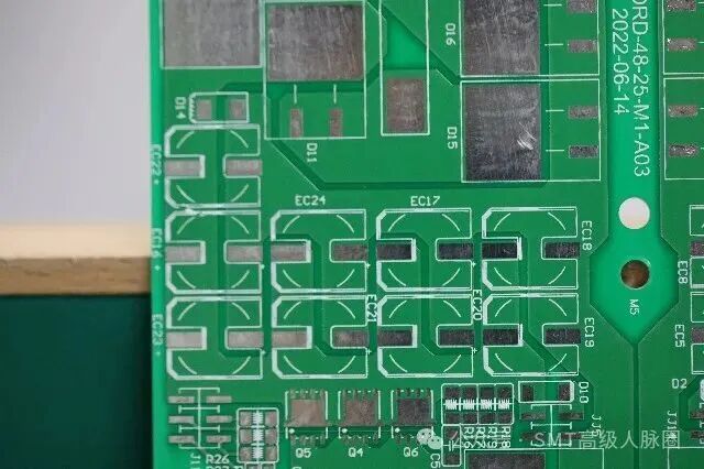
High-Frequency PCB Routing Techniques
1. Core Routing Principles
Multilayer Board Design
High-frequency circuits have a high level of integration and require at least a four-layer board (top layer, bottom layer, power layer, ground layer). The intermediate layers should be used for shielding and nearby grounding to reduce parasitic inductance, shorten signal transmission paths, and minimize cross-interference. For example, a four-layer board has 20dB lower noise than a double-sided board.
The power layer should be adjacent to the ground plane, utilizing plane capacitance filtering to enhance decoupling effects.
Lead Optimization
Length Control: High-frequency signal leads (such as clock, crystal oscillator, DDR data, LVDS, USB, HDMI, etc.) should be as short as possible to reduce radiation and coupling. The intensity of signal radiation is proportional to the length of the trace, and long leads are prone to coupling with adjacent components.
Bending Treatment: Leads should preferably be straight, using 45° bends or arcs when turning, avoiding right angles or sharp angles. In low-frequency circuits, bends are only used to enhance the adhesion strength of copper foil, while in high-frequency circuits, they can reduce signal emission and coupling.
Interlayer Via Reduction: The fewer vias used when connecting components, the better. Each via introduces about 0.5pF of distributed capacitance, and reducing the number of vias can significantly improve speed. For example, when changing layers for high-speed signal lines, grounding vias should be placed near the vias to provide a return path.
Crosstalk Prevention
Parallel Trace Control: Avoid running signal lines in close parallel proximity. If unavoidable, place a large area of ground on the opposite side of the parallel signal lines to reduce interference. When parallel traces on the same layer cannot be avoided, the routing direction on adjacent layers should be perpendicular.
Spacing Adjustment: Increase the spacing between signal lines to reduce parallel lengths. For example, the DDR bus must meet the “2W principle” (line spacing ≥ 2 times the line width) to reduce crosstalk.
2. Key Signal Processing
Differential Pair Routing
High-speed differential signals (such as LVDS, USB, HDMI) must be routed with strict equal length, equal spacing, and symmetry to maintain matched impedance (e.g., 100Ω±15%). The internal spacing of differential pairs should be small, while the external spacing should be large, avoiding the placement of components or vias between differential pairs.
Serpentine routing is used to equalize timing, but it increases parasitic capacitance, and the spacing should be ≥ 2 times the line width. For example, DDR3 signal lines need to use serpentine routing to compensate for length differences, ensuring signal synchronization.
Impedance Matching
During signal transmission, if there is an impedance mismatch, reflections occur, leading to signal overshoot or undershoot. It is necessary to ensure that the characteristic impedance of the transmission line matches the load impedance; for example, USB 3.0 signal lines should have an impedance controlled at 90Ω±10%.
Avoid abrupt changes or corners in transmission lines to maintain continuous impedance at all points. For example, high-speed signal line corners should use 135° bends to reduce signal reflections.
Signal Integrity Protection
Ground Enclosure: Important signal lines (such as clock, reset) or local units (such as crystal oscillators) should be surrounded by ground, and the outer contour line should be drawn to automatically generate a “ground enclosure” to reduce interference.
Avoid Loops: High-frequency signal routing should avoid forming loops. If unavoidable, minimize the loop area to reduce electromagnetic radiation.
3. Power and Ground Design
Decoupling Capacitor Layout
Add high-frequency decoupling capacitors (such as 0.1μF ceramic capacitors) next to the power pins of each integrated circuit block to suppress power harmonic interference. The capacitors should be placed close to the chip power pins, with values covering different frequency bands (e.g., 10μF + 0.1μF).
Add TVS diodes and fuses at the power entry point for over-voltage/over-current protection.
Ground Isolation and Connection
Isolate analog ground from digital ground: Analog and digital ground lines should be isolated using high-frequency choke beads or directly, with a single point interconnection to a common ground to prevent digital signals from interfering with analog signals. For example, place a single point connection between analog ground and digital ground under the ADC/DAC chip.
Grounding Strategy: Digital ground and analog ground should be connected at a single point under the chip or at the entry point, and the grounding method for mixed-signal chips should refer to the recommended scheme in the chip manual. In multilayer boards, the ground plane should be as complete as possible to avoid forming “islands”.
4. Layout and Process Optimization
Partitioned Layout
Analog circuits and digital circuits should be arranged in separate zones to avoid crossing. High-speed signal lines should preferably run on inner layers while ensuring the reference plane is complete. For example, in a DSP system, the DSP chip, clock circuit, reset circuit, and external memory should form a minimal system to reduce interference.
High-power devices (such as power chips) should be kept away from heat-sensitive components like electrolytic capacitors and crystal oscillators, and connected to the bottom layer ground plane for heat dissipation through multiple vias.
Process Details
Via Size Control: High-frequency signal vias should use small diameters (such as 8-12mil) to reduce parasitic inductance. Blind and buried vias can improve routing density but are more expensive and are typically used in high-end products.
Solder Mask Window Treatment: Heat dissipation pads should be clearly marked for solder mask openings to avoid green oil coverage and enhance heat dissipation.