Before discussing the boot process, let’s briefly talk about the learning path for digital ICs. There are many directions in digital IC design, including processor chip design, memory chip design, logic chip design, and so on. Ultimately, we find that digital chip systems generally encompass three functions: storage, transmission, and computation. The value of a digital chip is closely related to the number of these three functions it contains. Digital chip design, from simple to complex, requires comprehensive consideration of storage methods, external transmission I/O methods, and internal computation methods or state machine implementations. Returning to the topic, let’s see how the SOC system boots. Booting can be initiated directly from storage; it can be from internal ROM, SRAM, or external FLASH, PSRAM, DDR, SD cards, etc. Booting can also be initiated through I/O transmission, which can be serial ports, JTAG, USB, PCIe, networks, etc. Internally, to support multiple boot methods, simple configurations can be determined through pin settings, while complex methods may require the introduction of state machines. Let’s first look at the simplest MCU, reference this document, whose system structure is shown in Figure 1: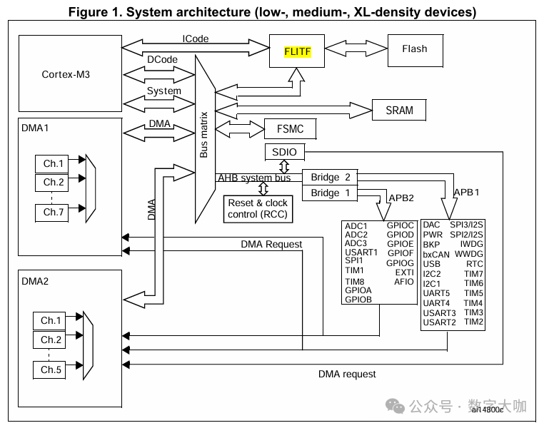 We can see that the M3 external connections include Icode, Dcode, and System, and the addresses of these buses are determined by the internal bus matrix of the M3. This internal bus matrix is roughly illustrated in Figure 2 (this is an illustrative example and does not match the above Figure 1):
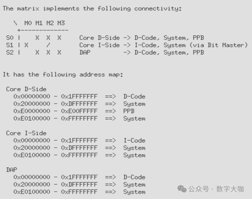 We can see that M0, M1, M2, and M3 correspond to the four CPU output masters, while S0, S1, and S2 are the three slaves of the bus matrix initiated by the three internal modules of the CPU. The bus matrix maps the operations of internal modules based on the addresses of the bus matrix into external master operations. Similarly, at the system level, there is also a bus matrix that converts the CPU’s external system bus operations into external I/O master operations, thus forming a complete system address space. It is worth noting that the bus matrix typically has a REMAP function, which can control the address mapping of the bus matrix through an input signal REMAP. This can be used during system boot to change the actual storage location from which the boot occurs. In Section 3.4, we find the boot configuration and boot modes, as shown in Figure 3:
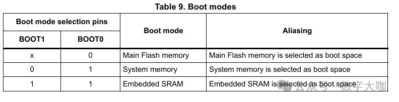 The system includes three modes, which can boot from the main Flash, system memory, or embedded SRAM. The mode selection is set by configuring the BOOT1 and BOOT0 pins, and after the chip powers on, it will automatically latch the BOOT pins. When exiting from StandBy mode, the BOOT pins will also be latched again. It is important to note that the clock for latching should be a free clock independent of the boot mode.After a boot delay, the CPU fetches the stack top value from address 0x0000 0000, and then starts executing code from the boot memory beginning at 0x0000 0004. Due to its fixed memory mapping, the code area starts from address 0x0000 0000 (accessed via the ICode/DCode bus), while the data area (SRAM) starts from address 0x2000 0000 (accessed via the system bus). The Cortex-M3 CPU always fetches the reset vector from the ICode bus, which means the boot space is only available in the code area (usually flash memory). The STM32F10xxx microcontroller implements a special mechanism, as mentioned earlier, the REMAP, which allows booting from SRAM, not just from the main Flash memory and System memory. In summary, there are generally two types of booting: Method 1: The program starts executing from internal ROM, with multiple branches depending on the supported boot modes. If it is the zero address of the main Flash, it starts running directly; if it is an external I2C or other peripheral boot mode, it needs to determine the current BOOT mode through the ROM program software code, run different initialization programs based on different boot modes, move the external boot program to internal storage, and then jump to the internal storage address 0x20000000 to start. Method 2: For external storage like PSRAM or NOR flash, after powering on, it can boot directly to zero address based on the BOOT mode through REMAP. If the PSRAM or NOR flash controller requires some configuration, it can be configured through Verilog hardware before the boot controller. For boot methods relying on internal ROM software code, since the ROM cannot be changed after the chip is fabricated, there is a certain risk that needs to be fully validated. Let’s briefly look at the boot process of the ZCU106, which contains an ARM A53 CPU and external DDR storage. Unlike microcontrollers, high-end CPUs generally run in external DDR after booting, considering capacity and speed. Reference this document. The boot process of the ZCU106 is relatively complex, managed and executed by the Platform Management Unit (PMU) and the Configuration Security Unit (CSU). The boot process includes three functional stages: pre-configuration stage, configuration stage, and post-configuration stage. The key programs run in PMU ROM, CSU ROM, and OCM, respectively. The pre-configuration stage is controlled by the Platform Management Unit, which executes PMU ROM code to set up the system. The PMU handles all reset and wake-up processes. Detailed processing is shown in Figure 4:
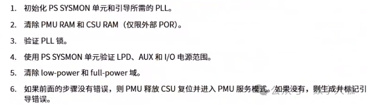 The configuration stage, BootROM (part of CSU ROM code) loads the first stage boot loader (FSBL) code into the on-chip RAM (OCM).The post-configuration stage, after the FSBL code starts executing in on-chip RAM, the CSU ROM code enters the post-configuration stage. The CSU ROM supports MultiBoot options, so a boot device can have multiple boot images. The boot image consists of a boot header file and partitions of different images along with their headers. Figure 5 shows the simplest form of a boot image, which contains only one mandatory image partition (FSBL) and the associated mandatory header.
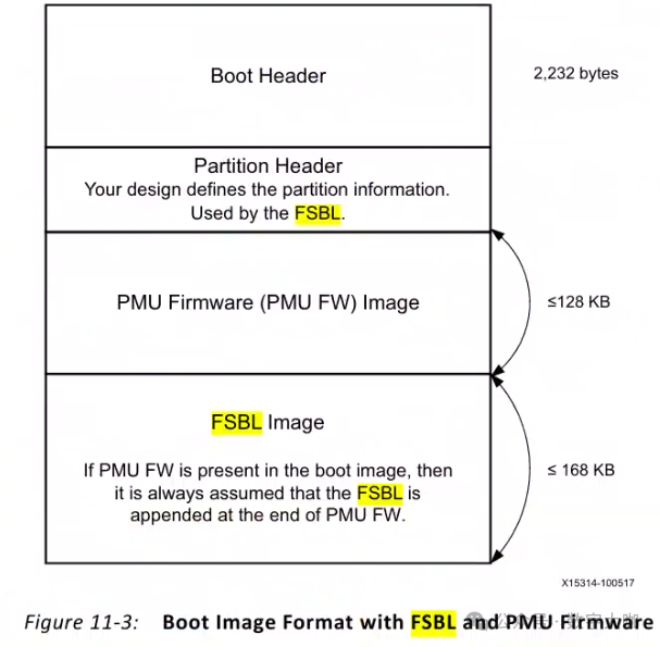 During the boot process, any errors from the CSU are recorded in the PMU_GLOBAL.CSU_BR_ERR register. Once an error occurs, this register logs a 16-bit error code, corresponding to two BootROM configuration error codes. Among them, [15-8] holds the first image error code, and [7-0] holds the most recent image error code. The specific format of the error code can be referenced in the manual Table 11-9. The boot processes of the MCU and CPU have been briefly introduced.In the future, we will continue to share SOC design insights. If you liked this article, feel free to follow the author.SOC Design (2) – RISC-V CPU Verilog ExecutionSOC Design (1) – Understanding Instruction Sets