
Via holes serve the purpose of connecting circuits, and the development of the electronics industry has also promoted the advancement of PCBs, which in turn raises higher requirements for PCB manufacturing processes and surface mount technology. The via hole plugging process has emerged to meet the following requirements:
(1) The via hole must contain copper; solder mask can be plugged or not;<br />(2) The via hole must contain solder, with a thickness requirement (4 microns), and must not have solder mask ink inside the hole, which could cause solder balls to be trapped inside;<br />(3) The via hole must be plugged with solder mask ink, opaque, and must not have solder rings, solder balls, or flatness requirements.As electronic products evolve towards being “light, thin, short, and small,” PCBs are also developing towards high density and high difficulty, leading to a large number of SMT and BGA PCBs. When customers require plugging during component mounting, there are five main functions:
(1) Prevent solder from penetrating through the via holes and causing short circuits during wave soldering; especially when vias are placed on BGA pads, plugging must be done first, followed by gold plating to facilitate BGA soldering.
(2) Avoid flux residue remaining in the via holes;
(3) After surface mount and component assembly, the PCB must be vacuumed on the testing machine to form negative pressure to complete the process;<br />(4) Prevent solder paste from flowing into the holes, causing cold solder joints and affecting mounting;<br />(5) Prevent solder balls from popping out during wave soldering, causing short circuits.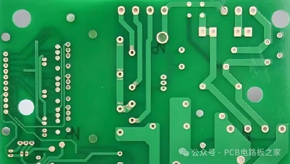
Plugging can be divided into resin plugging and electroplated plugging.
Resin plugging: Uses solvent-free ink for plugging, which not only addresses the issue of general inks being difficult to fill but also reduces the occurrence of “cracks” due to heat. It is generally used for larger diameter holes.
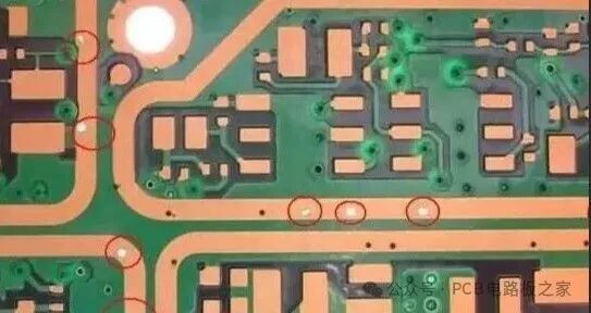
Benefits of resin plugging:
1. For via holes on multilayer boards with BGA, using resin plugging can reduce the spacing between holes, solving the issue of wiring and routing;
2. For buried holes in inner layer HDI, it can balance the thickness control of the laminated medium layer and the design of filling glue for inner layer HDI buried holes;
3. For thicker through holes in the board, it can improve product reliability;
4. The use of resin plugging in PCBs is often due to BGA components. Traditional BGAs may route vias to the back side between pads, but if the BGA is too dense to route vias out, direct drilling from the pad to another layer can be done, and then the hole can be filled with resin and plated to become a pad, known as the VIP process (via in pad). If vias are only made on the pad without using resin plugging, it can easily lead to solder leakage, causing short circuits on the back side and cold solder joints on the front side.
The process of PCB resin plugging includes drilling, electroplating, plugging, baking, and grinding. After drilling, the holes are plated, then resin is plugged and baked, and finally ground to a flat surface. The resin, being free of copper, requires an additional layer of copper plating to turn it into a pad. These processes are done before the original PCB drilling process, meaning the holes to be plugged are treated first, and then other holes are drilled, following the normal process.
If the plugging is not done well and there are bubbles inside the hole, the bubbles can easily absorb moisture, and when the board goes through the soldering furnace, it may cause board explosion. However, if there are bubbles during the plugging process, they will push the resin out during baking, causing one side to be recessed and the other side to be protruded. At this point, defective products can be identified, and boards with bubbles may not necessarily explode, as the main cause of board explosion is moisture. Therefore, if the boards are freshly manufactured or have been baked during the process, they generally will not cause board explosion.
Electroplated filling: Currently, it utilizes the characteristics of additives to control the growth rate of copper in various parts for filling. It is mainly used in the production of continuous multilayer stacked holes (blind hole process) or high current designs.
Advantages of electroplated filling:
1. Beneficial for designing stacked holes and plated through holes;
2. Improves electrical performance, aiding high-frequency designs;
3. Aids in heat dissipation;
4. Plugging and electrical interconnection are completed in one step;
5. Filling blind holes with electroplated copper provides higher reliability and better conductivity than conductive adhesives.
So,how is the PCB via hole plugging process achieved?
1. Plugging process after hot air leveling
This process flow is: board surface solder mask → HAL → plugging → curing. Using a non-plugging process for production, after hot air leveling, all vias to be plugged are completed using an aluminum sheet stencil or ink-blocking screen. The plugging ink can be photo-sensitive ink or thermosetting ink. This process flow ensures that the vias do not lose ink after hot air leveling, but it can easily cause ink contamination on the board surface and unevenness, leading to cold solder joints during mounting.
2. Plugging process before hot air leveling
1. Use aluminum sheets for plugging, curing, and grinding the board before graphic transfer
This process uses a CNC drilling machine to drill the aluminum sheets that need plugging, creating a stencil for plugging; the plugging ink can also be thermosetting ink, which has high hardness and good adhesion to the hole wall. The process flow is: pretreatment → plugging → grinding → graphic transfer → etching → board surface solder mask
This method can ensure that the via holes are plugged evenly, hot air leveled, and will not have oil loss or hole edge oil loss quality issues, but this process requires thick copper to be added at once, thus having high requirements for overall board copper plating.
2. Plugging with aluminum sheets followed by direct screen printing of the board surface solder mask
This process uses a CNC drilling machine to drill the aluminum sheets that need plugging, creating a stencil, which is installed on the screen printing machine for plugging. After completing the plugging, it should not be stored for more than 30 minutes, and the board surface solder mask is directly screen printed using a 36T screen; the process flow is: pretreatment → plugging → screen printing → pre-baking → exposure→ developing → curing.
This process can ensure that the vias are well covered with solder, the plugging is even, and after hot air leveling, it ensures that the vias do not get solder, and there are no solder balls trapped inside, but it can easily cause the ink to adhere to the pads after curing, leading to poor solderability.
3. Aluminum sheet plugging, developing, pre-curing, and grinding before board surface solder mask
Using a CNC drilling machine, drill the aluminum sheets that need plugging, creating a stencil, which is installed on a shift screen printing machine for plugging; the plugging must be full, protruding on both sides, and then cured and ground for board surface treatment. The process flow is: pretreatment → plugging → pre-baking → developing → pre-curing → board surface solder mask.
This process uses plugging curing, ensuring that the vias do not lose oil or explode after HAL; however, after HAL, the issue of solder balls being trapped in the vias and soldering on the vias is difficult to completely resolve.
4. Simultaneous completion of board surface solder mask and plugging
This method uses a 36T (43T) screen, installed on the screen printing machine, using a backing plate or pin bed, to plug all vias while completing the board surface; the process flow is: pretreatment → screen printing → pre-baking → exposure → developing → curing.
This process flow is short, with high equipment utilization, ensuring that the vias do not lose oil after hot air leveling and do not get solder, but due to using screen printing for plugging, a large amount of air remains in the vias, which expands during curing, breaking through the solder mask, causing voids and unevenness.


Some screenshots from electronic books

【Complete Set of Hardware Learning Materials Collection】