
With the continuous evolution of System-on-Chip (SoC) devices, modern electronic systems have gained unprecedented computing power while also presenting increasingly complex power distribution challenges.
Especially in the context of companies striving to accelerate time-to-market and control costs, optimizing the Power Delivery Network (PDN) has become a key factor in successful product development.

Author
Zach Caprai
Technical Market Engineer at Siemens, focusing on the HyperLynx analysis tool suite for PCB design.
This article demonstrates advanced PDN optimization methods through a real case study based on the AMD Versal adaptive SoC platform.
Utilizing the VCK190 evaluation toolkit equipped with the Versal AI Core series VC1902 device, it explores how effective PDN design and optimization can meet stringent technical specifications while achieving critical business objectives.

Understanding the Challenges of Modern PDN
Modern SoCs require precise power distribution across a wide frequency spectrum ranging from direct current (DC) to gigahertz (GHz).
The PDN must maintain stable voltage levels across the entire frequency range while managing current transients and minimizing impedance. This challenge is particularly complex for configurable devices like the AMD Versal adaptive SoC, as their power requirements can vary significantly with different configurations and applications.
The core voltage supply VCCINT (0.8 V) of the SoC must remain stable within a ±3% operating range, with 1% allocated for DC tolerance and 2% for AC voltage ripple. If the PDN performance is inadequate when the current load increases, it can lead to severe consequences.
Excessive voltage ripple caused by the PDN’s inability to maintain stable voltage levels can introduce noise and distortion, which in turn affects signal integrity.
More critically, unacceptable voltage drops can prevent key components from receiving the required voltage, leading to system instability, data corruption, or even complete failure.

The above is an advertisement and is not related to the main content.
These issues pose significant risks to device reliability and overall performance. Intermittent failures, data loss, and reduced lifespan are just some of the potential consequences of poor PDN design.
To mitigate these risks and ensure robust performance under harsh conditions, engineers must adopt advanced PDN design and optimization methods.
These include: precise analysis of power requirements; selection of appropriate components and topologies; and rigorous simulation and testing to validate the PDN’s ability to maintain stable power delivery under various operating conditions.
One of the critical parameters in PDN design and optimization is the target impedance. It defines the impedance threshold that the system must meet to maintain stable voltage levels.

Target Impedance Requirements
The voltage drop at the device power pins is caused by current flowing through the PDN with a certain impedance. To maintain a stable and consistent voltage at the device pins, the PDN’s impedance must always be below the predetermined target impedance Ztarget.
In the case of the Versal adaptive SoC, the device’s power consumption depends on the user’s configuration settings. As shown in Figure 1, AMD’s Power Design Manager (PDM) can be used to derive several key parameters for calculating the target impedance.
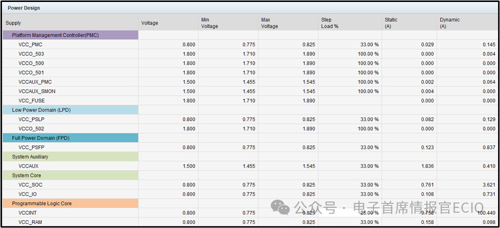
Figure 1: AMD software displays the dynamic current and step load percentage of the VCCINT power network.
In this case, the supply voltage is 0.8 V, with an allowable AC voltage ripple of 2%, combined with a maximum dynamic current of 100.440 A and a step load ratio of 25%, resulting in a calculated target impedance of 0.6372 mΩ. This precise target impedance must be maintained across a wide frequency range, especially in the critical frequency bands where decoupling capacitors are most effective.
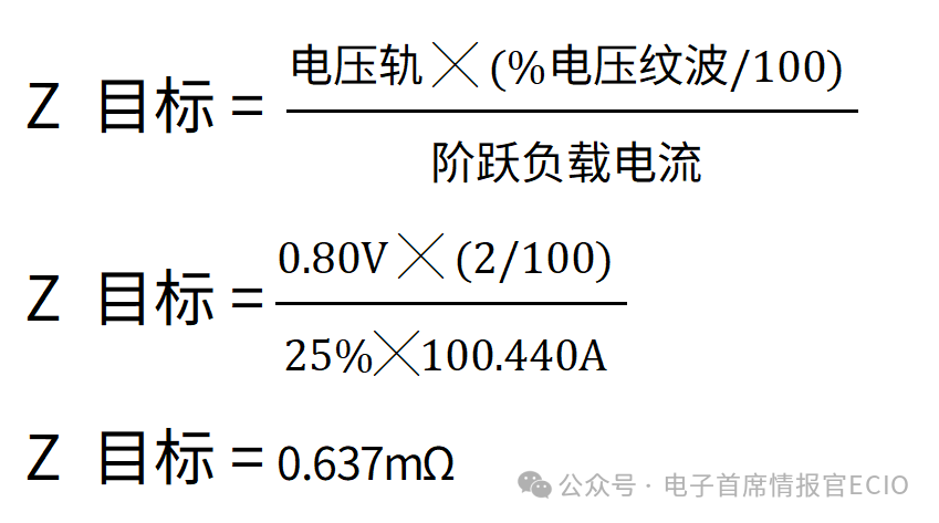
Once the target impedance is determined, the next step is to enter the PDN verification process. This critical step allows designers to assess the performance of the PDN design and ensure it meets the required technical specifications.

Verification Methods
The system’s verification methods need to model several key elements of the PDN.
First, model the Voltage Regulator Module (VRM) using a simplified resistor-inductor circuit to represent the output impedance seen by the PDN from the voltage regulator.
This model consists of resistance and inductance values that accurately reflect the behavior of the VRM within the frequency range of interest.
Next, it is necessary to characterize the decoupling capacitors. In this case, the VCCINT power network initially used 172 Murata decoupling capacitors. Each capacitor was modeled using resistor-inductor-capacitor (RLC) parameters extracted from the manufacturer’s specifications to account for parasitic effects that influence high-frequency behavior.
Many modern PDN tools also support SPICE models and S-parameter models for capacitors.
Once the models are specified, an IC pin group probe is constructed between the power and ground pins to observe the impedance at the device pins, ensuring that the target impedance requirements are met.
In the generated impedance curve (Figure 2), the red horizontal line indicates the calculated target impedance requirement of 0.637 mΩ, while the blue curve shows the PDN impedance curve composed of the PCB and decoupling capacitors.
Noticeable frequency-dependent behavior can be observed: below 1 MHz, it is primarily dominated by the VRM and bulk capacitance; in the 1-15 MHz range, local decoupling capacitors are most effective.
The current design meets the target impedance requirement below 12 MHz, with only a slight overshoot near 5 MHz. The resonance peak approaching 1 GHz is caused by the interaction between the power and ground layer capacitance.
The green curve shows the PCB PDN after connecting the AMD package model. After adding the package model, the PDN now meets the target impedance requirement within 19 MHz.
AMD recommends PCB designers modify the circuit board layout and PCB capacitor configuration to ensure that the PDN impedance meets the target impedance requirement in the 15-20 MHz frequency range.
For frequencies above 15-20 MHz, the decoupling capacitors inside the Versal device package will play a role in ensuring that the chip-level voltage remains within the appropriate operating range.
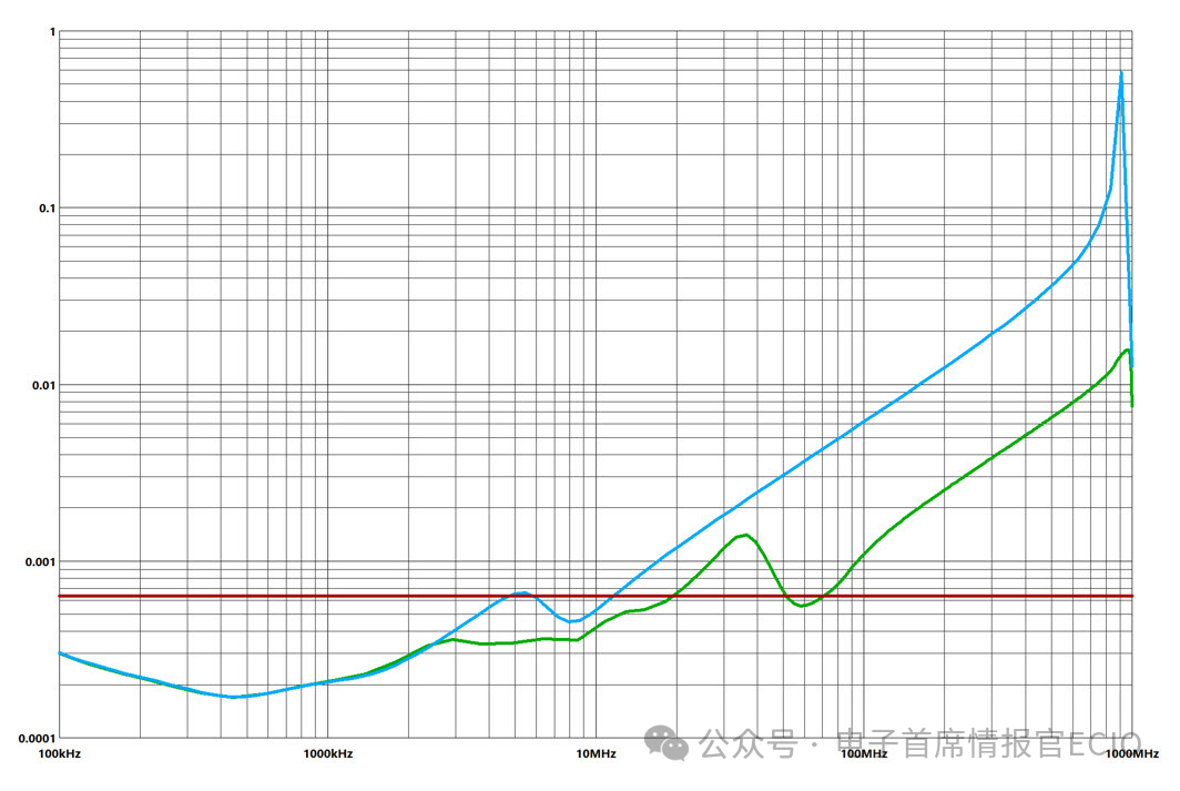
Figure 2: PDN impedance curves for PCB (blue) and package PCB (green).

Optimization Strategies
After establishing baseline PDN performance, designers can further explore optimization possibilities. Although the initial design followed AMD’s recommended configuration for the Versal adaptive SoC, there is still room for improvement in both performance and cost efficiency.
Current software tools, such as the HyperLynx PDN Decoupling Optimizer, employ two distinct yet complementary optimization methods.
The first method is a comprehensive approach, which provides a rapid iterative process based on established best practices. This method is particularly valuable in the initial optimization phase, allowing for quick identification of potential improvement points in the design.
The second method employs a Genetic Algorithm for more complex optimization. This method begins with the S-parameter model of the PCB PDN.
In this case, a 173-port S-parameter model is used, where port 1 represents the Versal device pin with the package model connected, serving as the observation point for impedance analysis; the remaining 172 ports correspond to the 172 potential decoupling capacitor installation locations on the circuit board.
The Genetic Algorithm considers multiple variables, including:
-
Selecting capacitors from the available component library;
-
Achieving optimal layout at installation locations;
-
Meeting target impedance requirements across the entire frequency range;
-
Cost constraints and component availability;
-
Capacitor package size and assembly process considerations.

Actual Results
The optimization process achieved significant improvements in both performance and cost efficiency. Although the baseline design itself was effective, it utilized 172 capacitors across 7 different part numbers. Through optimization, multiple alternatives with different advantages were generated.
As shown in Figure 3, two solutions stand out: the first optimization reduced the number of capacitors to 90 and the variety of part numbers to 6.
This configuration meets all performance requirements while reducing costs by 2.24%, despite having a relatively small performance margin.
Its PDN impedance curve touches the target impedance line at specific frequencies (2.5 MHz and 13.5 MHz) but remains within specification across the 15 MHz range.
To further explore design alternatives and potential improvements, a second optimization analysis was conducted, this time incorporating an additional 5% performance margin requirement.
This optimization run yielded an alternative solution using 111 capacitors. Compared to the baseline design, this configuration achieved a significant cost reduction of approximately 29.53% while providing a higher performance margin.
Although the second optimization solution used more capacitors than the first, it still resulted in greater cost savings due to the inclusion of lower-cost components in the input capacitor library.
This highlights several key factors that need to be balanced in PDN design: cost reduction, total component count, and available routing space.
These trade-offs depend on the specific capacitor types chosen in the design. Additionally, increased design margins are particularly valuable for designs that require high reliability under varying operating conditions.
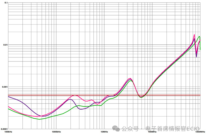
Figure 3: PDN impedance curve comparison showing PCB/package baseline (green), optimization run 1 (red), and optimization run 2 (purple).

Practical Design Considerations
The optimized design solutions highlight several key practical considerations in PDN design. Side capacitors installed directly beneath the device, when positioned close to the power and ground pins of the ball grid array, prove particularly effective.
This strategic layout maximizes the effectiveness of the capacitors by effectively shortening the current path length and reducing loop inductance.
Understanding the frequency-dependent characteristics of decoupling capacitors is crucial for achieving effective optimization. Below their self-resonant frequency (SRF), capacitors exhibit a typical negative slope impedance curve—i.e., impedance decreases as frequency increases.
However, when the frequency exceeds their self-resonant point, the behavior of the capacitors is dominated by inductive characteristics, and the impedance curve shows a positive slope trend. This characteristic makes the selection and layout of capacitors critical for maintaining target impedance across the entire target frequency range.
During the optimization process, special attention must be paid to the parallel resonance frequency (PRF) point.
When multiple capacitors interact, they can create high impedance peaks in the PDN’s impedance curve, which can undermine the core design goal of maintaining low impedance within the target frequency range.
To meet target impedance requirements, it is essential to provide a capacitor component library that includes a variety of capacitor values.
This diversity allows the optimizer algorithm to select the most appropriate components for the design while fully considering the interactions of parallel resonant frequencies between different capacitors.
Additionally, the capacitor component library should only include components from qualified suppliers. If the library contains discontinued or unapproved parts, the optimization tool may generate results that include undesirable or unobtainable components, potentially leading to issues in the final design.

Comprehensive Reporting
Modern PDN decoupling analysis tools can generate comprehensive reports that help engineers make informed decisions about their power distribution network designs.
One key feature is the loop inductance analysis for each capacitor mounting location, used to identify potential layout improvement opportunities for better performance.
The optimization process considers the behavior characteristics of the PDN across the entire frequency range:
-
DC to 100 kHz: Primarily dominated by the performance of the Voltage Regulator Module (VRM) and bulk capacitance;
-
100 kHz to 15 MHz: The critical frequency range for local decoupling capacitors;
-
Above 15 MHz: Transitioning to package-level and chip-level decoupling.
For each design solution, the optimization tool provides detailed design recommendations, including the best capacitor selection for each component mounting location.
For capacitor locations deemed unnecessary, the tool will mark them as “open” in the termination bar, achieving cost reduction and simplifying circuit board routing while still meeting the design requirements for target impedance.
The tool can analyze the complete frequency range, which is particularly important for high-performance devices like the Versal adaptive SoC, whose performance requirements span a wide spectrum from DC to GHz.

Flexibility in Adapting to Multiple Design Configurations
Another significant advantage of the optimization process is its ability to adapt to different programmable device images (PDI) deployed on the same hardware.
Each PDI may have different dynamic power requirements and step load characteristics while providing various functionalities and performance levels.
Today’s design tools enable engineers to optimize their step load response for specific PDI needs while maintaining the same circuit board layout and using different bills of materials.
This flexibility is also reflected in support for multiple optimization objectives. While this case study primarily focuses on cost reduction, the same methods can be applied to achieve other optimization goals, such as:
-
Maximizing performance margin
-
Minimizing component count
-
Reducing circuit board space usage
-
Improving manufacturing efficiency
The optimization process balances electrical performance requirements with manufacturing process needs. Reducing the number of component types from 7 to 6 may seem trivial, but this change can significantly impact inventory management and assembly processes.
Using a standard supplier component library during the optimization process ensures component availability.

Conclusion
As SoC devices continue to evolve, their power distribution requirements will become increasingly stringent.
The methods presented in this article provide a scalable optimization framework to address future challenges, accommodating the needs of new devices and supporting designs across various power domains.
Through PDN optimization, seemingly contradictory goals can be achieved—enhancing performance while reducing costs.
The ability to reduce component counts by nearly 50% while maintaining or even improving system performance demonstrates the powerful potential of advanced optimization methods.
This approach becomes particularly important against the backdrop of rising operating frequencies and increasingly stringent power demands.
Collaboration between chip suppliers and EDA tool vendors has built a comprehensive ecosystem that enables engineers to stay at the forefront of evolving design requirements.
AMD provides detailed S-parameter models for all Versal product lines, combined with advanced optimization tools, ensuring designers can effectively tackle future challenges.
Successfully optimizing the PDN ultimately depends on finding a balance among various conflicting factors: electrical performance, cost efficiency, manufacturability, and design configuration flexibility.
Modern design tools provide engineers with the capabilities needed to effectively achieve this balance, enabling them to develop robust PDN solutions that meet current needs while addressing future power distribution challenges.
For more information, click below to read the original article and the related white paper published by Siemens EDA.









Above are the electronic chief intelligence officer partners(partial)
Order does not indicate priority