👇Click to follow for daily technical insights!👇
1 Introduction
SPI: Serial Peripheral Interface, a serial peripheral interface.
SPI was developed by Motorola around 1985 and is a synchronous serial interface suitable for short-distance, device-to-device communication.
Since then, this interface has become a de facto standard adopted by many semiconductor manufacturers, especially microcontrollers (MCUs) and microprocessors (MPUs).
2 SPI Interface
The SPI bus is a 4-wire bus, typically consisting of one master device and one or more slave devices, requiring at least 4 wires, although 3 can suffice.
MOSI: Master Output Slave Input, data output from the master device to the slave device;
MISO: Master Input Slave Output, data input to the master device from the slave device;
SCLK: Serial Clock, the clock signal generated by the master device;
SS: Slave Select, the signal to select the slave device, controlled by the master device;
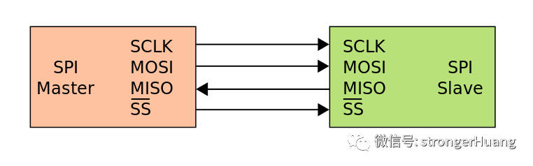
The above SS signal can also be understood as the CS signal, generally active low, hence also referred to as the NSS (not) signal;
CS: Chip Select, the chip select signal (slave device enable/select signal), controlled by the master device;
One Master One Slave
The most basic SPI communication involves one master and one slave, for example: an STM32 as the master and a W25Q16 (SPI Flash) as the slave. SPI communication can also occur between two MCUs.
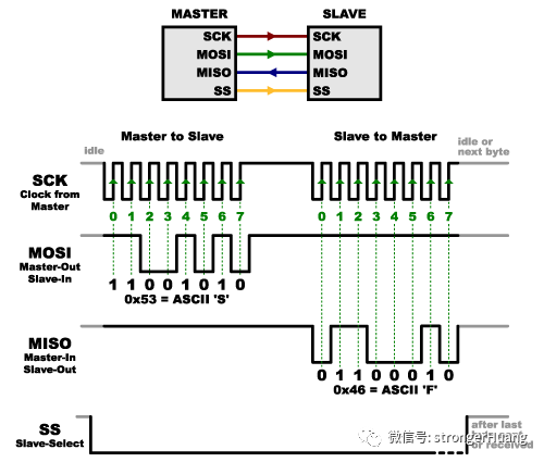
The example above shows the master sending one byte of data (0x53), and the slave responding with one byte of data (0x46).
One Master Multiple Slaves
SPI can support one master and one slave (one master, one slave), but it can also support one master and multiple slaves. There are two common connection methods for one master and multiple slaves.
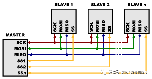
A. Conventional
Typically, each slave requires a separate SS line; to communicate with a specific slave, set that slave’s SS line to low while keeping the others high.
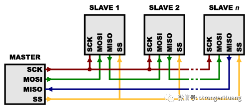
B. Single SS Signal
Some applications only require one NSS (e.g., shift registers); in this layout, data is shifted from one slave device to another.
3 SPI Data Transmission
SPI communication is relatively simple, with one clock transmitting one bit of data (master -> slave, or slave -> master).
SPI Clock
Theoretically, the clock frequency of SPI can be very high, typically ranging from a few MHz to several hundred MHz. For the commonly used W25Q16, SPI supports a maximum of 80MHz.
The SPI communication speed must be combined with actual conditions and cannot exceed the maximum clock frequency supported by the master or slave.
SPI Data
SPI data flows in two directions:
MOSI: Master -> Slave
MISO: Slave -> Master
One drawback of SPI communication is that there is no specified flow control and no acknowledgment mechanism to confirm whether data has been received.
This can be understood as: it is unclear when the master sends data to the slave, when the slave sends data to the master, and how many bytes of data should be sent.
At this time, the communicating master and slave must reach an agreement, generally with the master controlling read and write operations.
For example, the following operation reads and writes data to the SPI Flash:
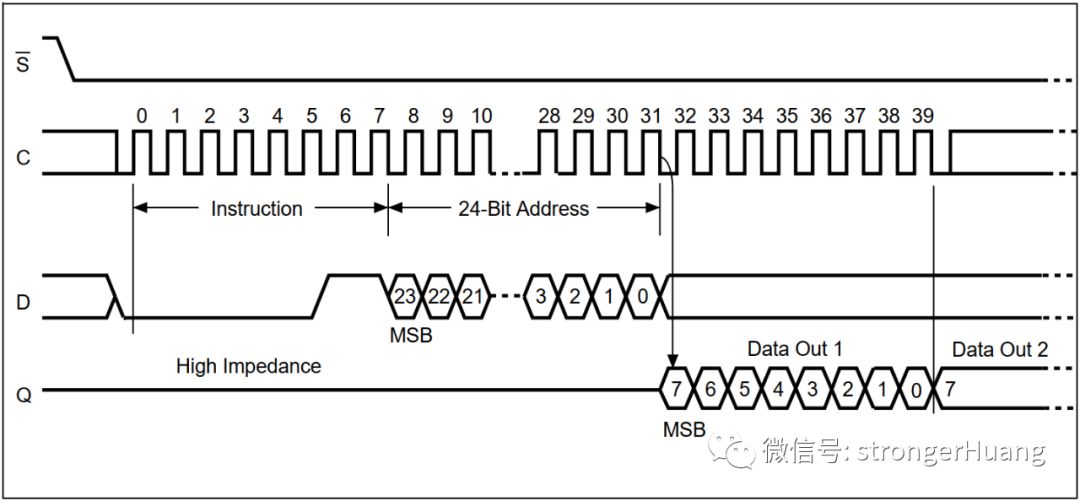
The first byte is the instruction, followed by 3 bytes (24 bits) of address, all sent from the master to the slave. After that, the master reads data (sent by the slave).
Clock Polarity and Phase
In addition to setting the clock frequency, the master must also configure the clock polarity and phase related to the data.
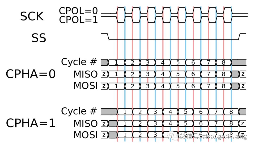
CPOL determines the clock polarity, which can be converted using a simple inverter.
CPHA determines the timing of the data bits relative to the clock pulse (i.e., phase).
Generally, processors with integrated SPI peripherals have SPI-related configuration registers; for STM32, detailed information about SPI configuration can be found in the reference manual.
It is recommended to understand this in conjunction with timing diagrams rather than rote memorization.
Statement: The article is authorized and adapted from “strongerHuang”, copyright belongs to the author. If there is any infringement, please contact us for deletion!— End —
Recommended Reading
Detailed Explanation of CAN Protocol Signal Packet Is Actually Worse? A Low-Cost FOC Control Solution Does Electric Soldering Iron Have Toxicity?  Brothers, please like, view, and share👇Good content needs your support!