Click the blue text to follow us
Printed Circuit Boards
In the early 20th century, Paul Eisler first proposed the concept of “printed circuits” and developed the world’s first printed circuit board (PCB). As the most widely used substrate in secondary electronic packaging technology, it is a substrate covered with single or multiple layers of wiring, used to support and connect components to form specific functional modules. Common types include rigid, flexible, metal-clad, and injection-molded boards. Except for special types, they are usually made of glass fiber reinforced polymer resin boards coated with copper foil circuits. The manufacturing process integrates various technologies and has made significant progress in many areas, achieving a packaging density that is a hundred times higher than before. They can also be classified into single-sided, double-sided, and multilayer printed circuit boards based on the number of conductor circuit layers.
This article follows the main process of “drilling – metallization – patterning – lamination – coating – forming” to introduce new technologies such as deep hole electroplating, black hole technology, and vacuum lamination.
1
Professional Principles of Multilayer PCB Design
In the field of PCB manufacturing, multilayer PCB substrates, while based on single-layer manufacturing technology, resemble ordinary single-layer boards before lamination. However, after lamination, due to the large and complex scale of circuit wiring, more functions need to be realized while meeting higher performance requirements. The wiring density significantly increases, with reduced line width and spacing, and stringent requirements for pattern accuracy. Additionally, precise through-hole connections between layers add to the manufacturing difficulty, far exceeding that of ordinary PCB substrates.
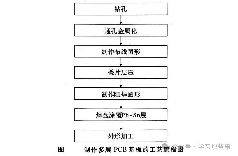
However, its general manufacturing process still follows an established pattern, covering key steps such as drilling, through-hole metallization, patterning, lamination, solder mask patterning, pad coating with Pb-Sn layers, and contour processing.
When designing multilayer PCBs, adhering to professional principles is crucial. To effectively reduce inter-layer interference, especially in high-frequency applications, adjacent layer routing should be arranged perpendicularly. The power layer should be placed on the inner layer, and its distance from the ground layer and the upper and lower signal layers should be close and evenly distributed. This layout not only avoids interference from long power lines on signal transmission but also prevents external factors from affecting power stability.
With the iterative upgrade of information technology, new packaging technologies have emerged rapidly, and electronic devices are accelerating towards lightweight and miniaturization, pushing PCB substrates towards ultra-thin multilayer boards. These types of PCBs feature narrow spacing, small apertures, fine line widths, and blind holes, presenting numerous challenges for manufacturing processes and giving rise to a series of new technologies.
2
Key Manufacturing Technologies for PCBs
Use of Thin and Ultra-Thin Copper Foils
In terms of copper foil selection, traditional multilayer PCBs often use copper foils with thicknesses of 18μm or 35μm, while ultra-thin multilayer boards, to meet the demands for fine line widths and narrow spacing (0.10mm or 0.05 – 0.08mm), often use thin copper foils with thicknesses below 18μm, such as 9μm or even 5μm. The reason is that for fine narrow lines, if several microns of pinholes occur during the photolithography process, thick copper foils are prone to severe lateral corrosion during etching, leading to line breakage, increased impedance, and severely affecting transmission performance and reliability; thin copper foils, on the other hand, have less lateral corrosion and can significantly improve line consistency.
Small Hole Drilling Technology
Small hole drilling technology is also a key aspect. Given the small aperture, high density, and stringent positioning accuracy requirements of multilayer PCBs, advanced drilling methods must be employed. CNC high-speed drilling, punching, and laser drilling have become mainstream choices. For substrates with thicknesses far less than 0.1mm and embedded holes, punching is more suitable from an economic cost perspective; while for through-holes after lamination, CNC drilling is typically used to ensure the quality of multilayer board processing. It is worth mentioning that in recent years, with the deep integration of artificial intelligence and automation technology, intelligent CNC drilling equipment has continuously emerged, capable of achieving more precise positioning and drilling control, further enhancing the efficiency and quality of small hole drilling.
Small Hole Metallization Technology
Small hole metallization technology also faces challenges and breakthroughs. As the aperture shrinks, the difficulty of metallization increases, and the process technology needs continuous upgrading. The drilled multilayer boards need to undergo decontamination treatment, and traditional strong acid and strong alkali decontamination methods are ineffective. Plasma methods and alkaline potassium permanganate decontamination technology have emerged. Under the influence of high-frequency and high-voltage electric fields, gases such as N₂, O₂, or CF₄, introduced after vacuuming, are ionized into plasma gases with strong chemical reactivity. Placing the drilled multilayer boards in this environment allows the contaminants on the hole walls to react with the plasma, creating favorable conditions for small hole metallization. Additionally, recent research teams in the industry have explored the application of new nanomaterials in the small hole metallization process, aiming to further enhance the uniformity and adhesion of the metallization layer, providing new ideas and directions for the high-performance development of multilayer PCBs.
Deep Hole Electroplating Technology
Deep hole electroplating technology is crucial for achieving high-quality metallization of embedded and through holes, with expectations for the plating layer to have a certain thickness, low resistance, and smooth hole walls. However, the fine and deep characteristics of small holes pose significant challenges to the metallization process. In recent years, black hole technology and direct metallization of holes (DMS) technology have emerged. Black hole technology uses conductive carbon powder to create a water-soluble suspension that is uniformly coated on the hole walls to make them conductive, thereby obtaining a uniform electroplating layer. Its process includes drilling, deburring, cleaning, hole finishing, washing, black hole treatment, oxidation resistance treatment, secondary washing, drying, and overall board electroplating. DMS technology first uses a potassium permanganate solution to oxidize the non-metallic hole walls, generating a MnO₂ layer, followed by organic monomer catalysis or activation treatment, uniformly coating the organic monomer film on the hole walls, and then placing it in a dilute H₂SO₄ solution to form a polymer conductive film containing salts through oxidative polymerization. Its process includes drilling, deburring, hole finishing, washing, micro-etching, secondary washing, oxidation, third washing, catalysis, fixation, fourth washing, and overall board electroplating. Notably, recent research teams have innovated based on black hole technology, attempting to introduce new nanoconductive materials to replace traditional conductive carbon powder, aiming to further enhance the uniformity and stability of hole wall conductivity, thereby optimizing electroplating layer quality.
Fine Line Pattern Etching Technology
Fine line pattern etching technology has also made significant progress. Traditional PCB layer boards use thick dry film resist for photolithography and etching wiring patterns, which is limited by film thickness and process constraints, resulting in low resolution of dry film resist, only capable of producing wiring patterns above 0.15mm. Liquid photoresists and electro-deposited photoresists effectively compensate for this shortcoming, with liquid photoresists capable of etching wiring patterns of 0.10mm and electro-deposited photoresists achieving fine etching of 0.05 – 0.08mm. To obtain finer wiring patterns, the surface treatment step is also crucial. Using pumice grinding technology instead of abrasive nylon brush grinding can achieve a more uniform and detailed surface, providing a good foundation for fine line etching. Recently, a new plasma-assisted etching technology has emerged in the industry, utilizing plasma to pre-treat the surface, further cleaning it and improving its surface roughness, which helps enhance the precision and consistency of fine line etching.
Vacuum Lamination Technology
Vacuum lamination technology has unique advantages in multilayer board manufacturing. During the heating and pressing of the semi-cured adhesive between layers, low molecular volatiles and adsorbed gases will escape. Under conventional lamination conditions, a small amount of volatiles or bubbles may remain between layers, affecting the flatness of multilayer boards and potentially causing misalignment of interlayer circuits. Vacuum lamination technology can effectively solve these problems; it not only reduces lamination pressure but also facilitates the easier expulsion of low molecular volatiles and bubbles, reducing resin flow resistance and significantly minimizing thickness deviations of laminated boards, which is significant for producing multilayer boards with fine wiring patterns. Recently, a new intelligent vacuum lamination device has been developed, capable of real-time monitoring of parameters such as pressure, temperature, and vacuum during the lamination process, and automatically adjusting based on actual conditions, further improving the quality and stability of vacuum lamination.

Currently, PCB substrate technology is rapidly developing but still faces many challenges. The trend towards miniaturization and high performance of electronic devices, along with decreasing pin spacing, and the gradual popularity of new packaging forms such as BGA and CSP, place higher demands on PCB technology. Traditional epoxy glass PCBs, due to their high dielectric constant and long signal delay times, struggle to transmit high-speed signals. The mainstream PCB spacing is 0.2 – 0.25mm, and producing below 0.1mm spacing significantly increases costs and makes yield difficult to guarantee. Additionally, traditional PCBs face prominent heat dissipation issues and serious environmental pollution problems during the manufacturing process, necessitating the adoption of environmentally friendly substrate materials.
To address these challenges, the industry is actively developing new technologies and processes. In small through-hole processing, chemical methods or laser technology are being explored; previously, PCB lines and spacing relied on photolithography methods, but laser direct imaging (LDI) technology has emerged, which controls LDI to directly draw patterns on a layer of PCB coated with photoresist through CAD/CAM systems, improving labor productivity, shortening design and production cycles, and achieving full automation from design to production, ensuring product quality. Additionally, Panasonic’s completely internal via (ALIVH) technology can achieve high density, fewer layers, and simplified designs for PCBs, providing a comprehensive solution to many issues faced by PCBs. Recently, research institutions have expanded studies based on ALIVH technology, exploring how to further optimize via structures and materials to enhance the electrical performance and reliability of PCBs, paving new paths for the future development of PCB technology.
To learn more and enjoy more benefits, you can join our knowledge community, where you can ask questions, and we will do our best to help you!


To facilitate communication among peers, this public account has created a series of technical discussion groups, and all colleagues are welcome to join! You can add the group owner on WeChat (WeChat ID: xxnxs999) to apply for group membership!
① Chip Packaging Process Discussion Group
② Failure Analysis and Reliability Discussion Group
③ Quality System Control Discussion Group
④ Advanced Packaging Process Discussion Group
⑤ Wafer Manufacturing Process Discussion Group
⑥ Analog Circuit Design Discussion Group
⑦ Wire Bonding Process Discussion Group
⑧ Packaging Equipment Technology Discussion Group
⑨ Electronic Assembly Technology Discussion Group
⑩ Thinning and Dicing Technology Discussion Group
You can reply to “join group” in the background or scan the group owner’s WeChat below to apply for group membership.

That’s all for sharing. If you have any needs, please leave a message in the background!

Learning About Those Matters