A Comprehensive Guide to Implementing I2C Master Core with FPGA (Part 5): Bit Counting & Byte Counting in Data Transmission

A Comprehensive Guide to Implementing I2C Master Core with FPGA (Part 5): Bit Counting & Byte Counting in Data Transmission

▼ Follow for more valuable insights “ On the journey of designing the I2C controller, we have successfully established the clock skeleton (SCL) and the command center (state machine). However, to truly make the data “move” and accurately control the transmission of each bit and byte, we need two key “counters”. This article will delve … Read more


Core Guide to Implementing I2C Master on FPGA (Part 2): Module Interface Design

▼ Follow for more valuable content “ Modern FPGA design typically adopts a “top-down” approach. We design the I2C master controller starting from the top-level functionality and interfaces. So how do we begin from the top-level design, gradually decompose the functionality, define the interfaces, and ultimately implement an I2C controller that supports multi-byte read/write, error … Read more

Challenges in FPGA Syntax

The “syntax” of FPGA (Field Programmable Gate Array) essentially refers to the rules for using hardware description languages (HDL, such as Verilog and VHDL) and associated design tools to describe hardware circuit logic. Compared to software programming languages (like Python and C++), the core difficulty of FPGA syntax arises from the conflict between its “hardware … Read more

Commonly Asked Questions in FPGA Interviews

Commonly Asked Questions in FPGA Interviews

In FPGA (Field Programmable Gate Array) interviews, questions typically revolve around fundamental principles, design processes, hardware description languages, timing analysis, and practical applications. 1. Basic Concepts and Structure What is the difference between FPGA and CPLD? Structure: FPGA is centered around CLB (Configurable Logic Block), containing numerous LUTs (Look-Up Tables) and registers, with abundant routing … Read more

Is the Chip Ready for Tape-Out Once the Verilog Code is Completed?

Is the Chip Ready for Tape-Out Once the Verilog Code is Completed?

If you want to create a SoC chip, self-develop customized IPs to highlight differentiation, and purchase other general-purpose IPs, then connecting them is all that is needed. Making an SoC is just about connecting the dots. Once the Verilog code is done, can the chip be sent for tape-out? Let’s not even talk about the … Read more

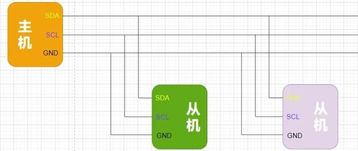
I2C Driver for FPGA Function Module

I2C Driver for FPGA Function Module

1. Introduction to I2C Reference Source https://blog.csdn.net/Teminator_/article/details/141224886 1.1 Overview of I2C Bus (1) The IIC protocol (Inter-Integrated Circuit, abbreviated as I2C) is a serial communication protocol used for communication and data exchange between various electronic devices. It was first proposed and promoted by Philips in 1982 as a simple, efficient, and low-cost communication protocol. (2) … Read more

Introduction to FPGA: Implementing Shift Registers with Verilog/VHDL

Introduction to FPGA: Implementing Shift Registers with Verilog/VHDL

What is a shift register? In FPGA (or ASIC), a shift register is a very common basic module. Its essence is to connect multiple flip-flops (registers) in a chain. All flip-flops share the same clock signal, and the output of each flip-flop is connected to the input of the next flip-flop. In this way, data … Read more

W25Q64 SPI Read/Write Control in Verilog for Gowin

W25Q64 SPI Read/Write Control in Verilog for Gowin

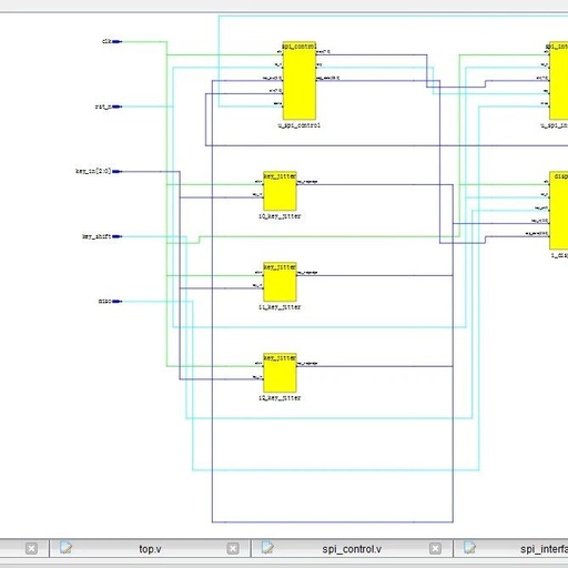
**Name:** W25Q64 SPI Read/Write Control in Verilog for Gowin **Software:** Gowin IDE **Language:** Verilog **Code Functionality:** Implements read/write operations for the W25Q64 SPI Flash, ID reading, and data display, controlled by buttons for read/write operations and a seven-segment display, suitable for embedded storage systems. **Code Implementation Approach:** This design implements SPI Flash read/write control in … Read more

Is the Chip Ready for Tape-Out Once the Verilog Code is Completed?

Is the Chip Ready for Tape-Out Once the Verilog Code is Completed?

If you want to create a SOC chip, self-develop customized IPs to highlight differentiation, while purchasing general-purpose IPs and simply connecting them, making a SOC is just about connecting the dots. Once the Verilog code is finished, is the chip ready for tape-out? Let’s not even discuss the technology of connecting the SOC; what happens … Read more

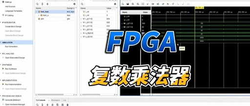
FPGA Tutorial Case 12: Design and Implementation of a Complex Multiplier Based on Vivado IP Core

FPGA Tutorial Case 12: Design and Implementation of a Complex Multiplier Based on Vivado IP Core

01Design and Implementation of a Complex Multiplier Based on Vivado IP CoreIn the fields ofdigital signal processing and image processing, complex multiplication is often required. A complex multiplier is a core component for performing this operation. Particularly in digital signal processing, complex multiplication has numerous applications, including signal mixing, FFT, and IFFT. The complex multiplier … Read more