**Name:** W25Q64 SPI Read/Write Control in Verilog for Gowin
**Software:** Gowin IDE
**Language:** Verilog
**Code Functionality:** Implements read/write operations for the W25Q64 SPI Flash, ID reading, and data display, controlled by buttons for read/write operations and a seven-segment display, suitable for embedded storage systems.
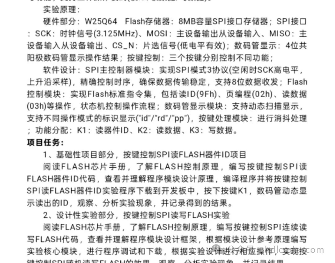
**Code Implementation Approach:**
This design implements SPI Flash read/write control in a modular manner. The top-level module collects user input through button debouncing, the SPI control module generates read/write requests, the SPI interface module is responsible for timing communication with the Flash, and the display module provides real-time feedback on operation status. The overall design uses a state machine to ensure a clear and reliable operation flow, with coordinated modules that facilitate expansion and debugging.
This code has been validated on a development board.
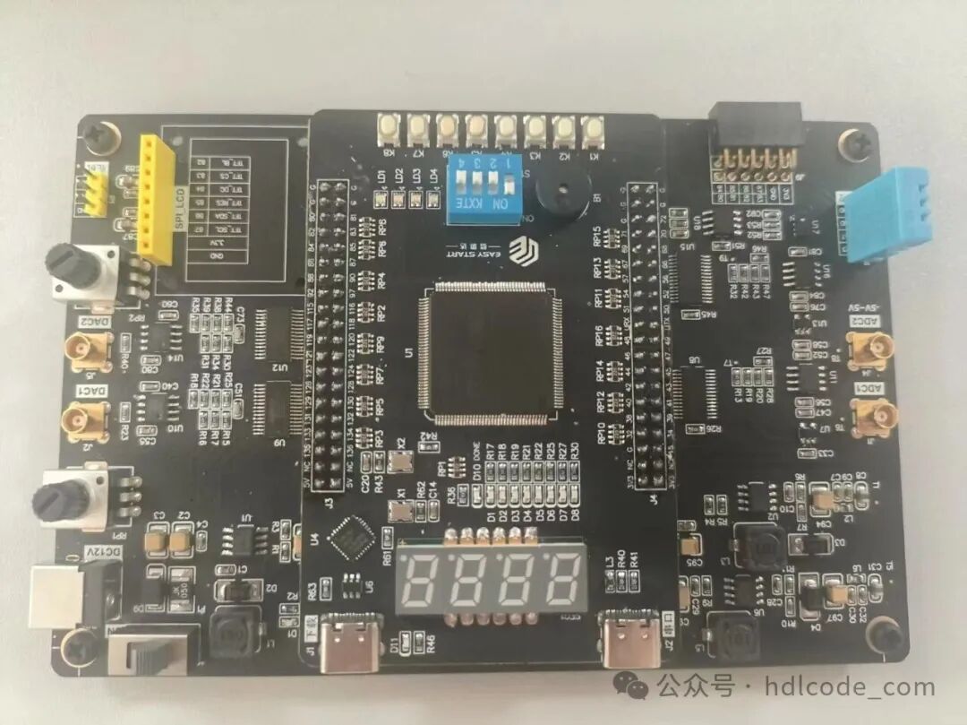
**Code Structure:**
– top: Top-level module that coordinates all functional modules for overall control.
– key_jitter: Button debouncing module that provides stable button signals.
– spi_control: SPI read/write control module that generates data read/write requests.
– spi_interface: SPI interface module that implements data timing communication with the Flash.
– spi_read_ctrl: Read control module that implements reading of Flash ID and data.
– spi_write_ctrl: Write control module that implements data writing and erasing operations.
– display: Seven-segment display module that shows the current operation status in real-time.
1、 Project Files
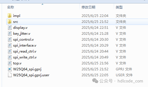
2、 Program Files
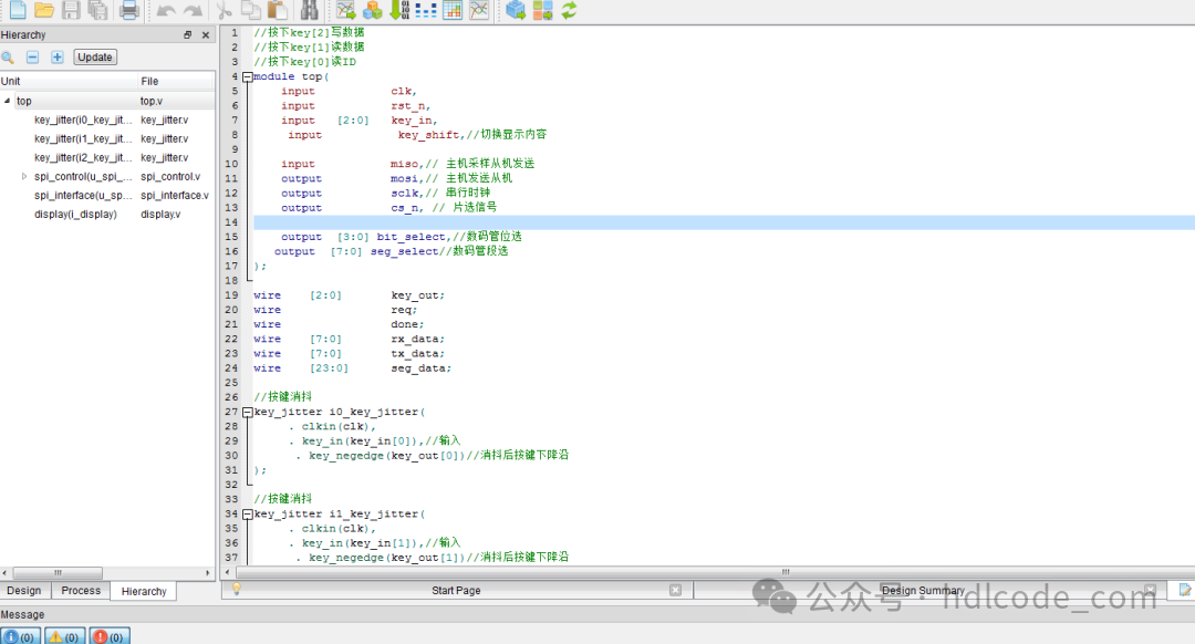
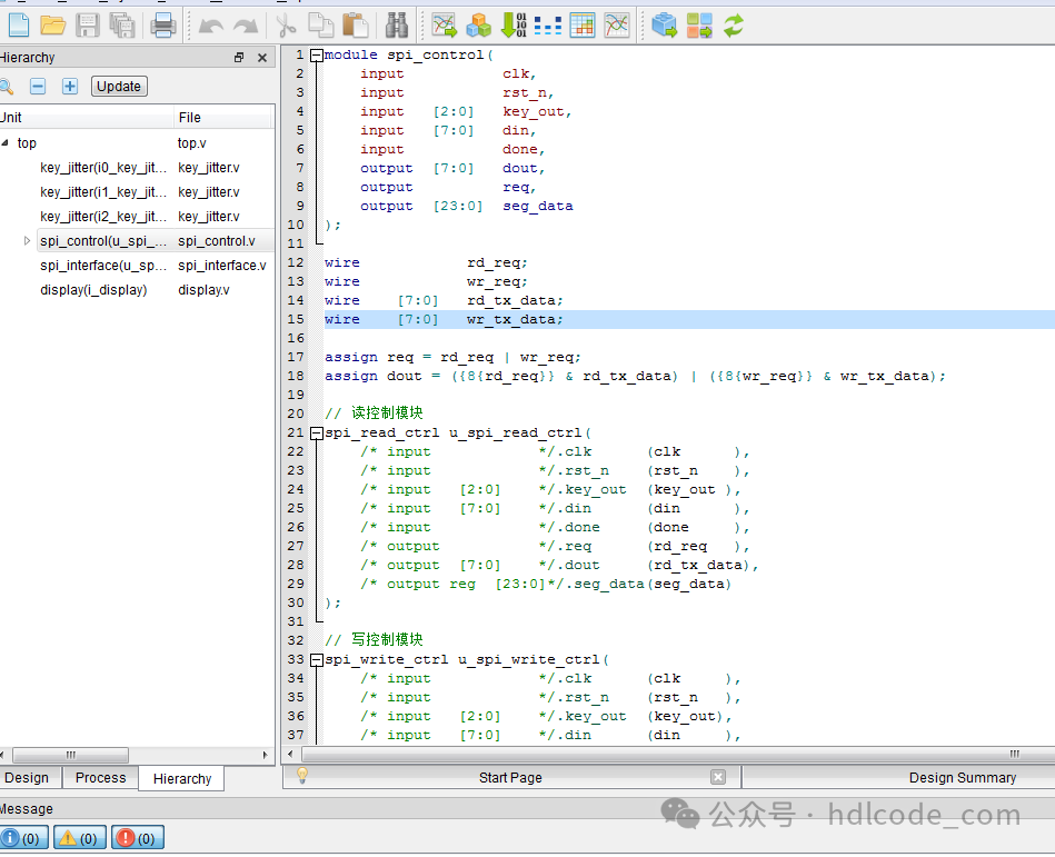
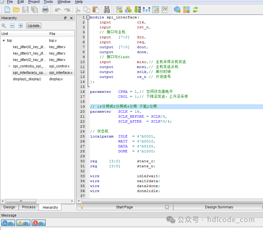
3、 Program Compilation
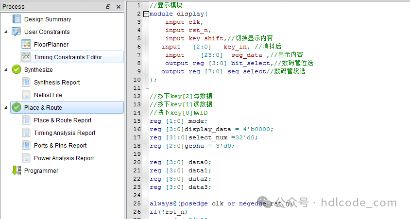
4、 RTL Diagram
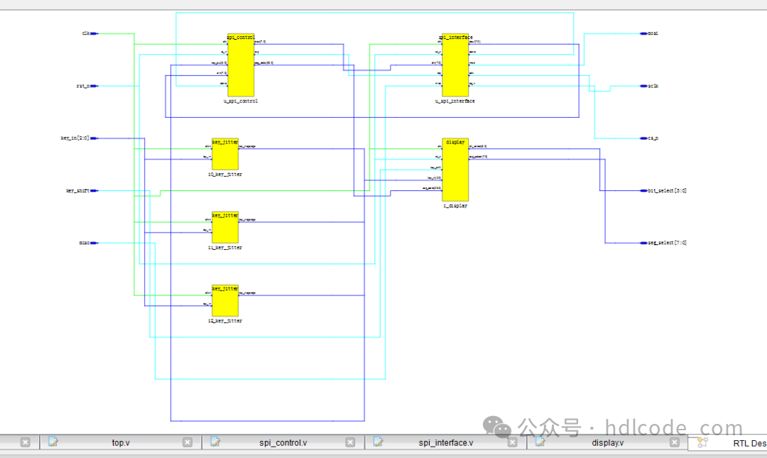
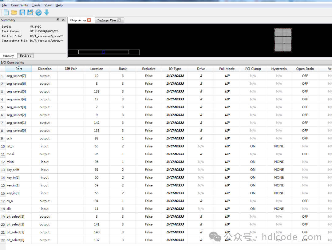
5、 Pin Assignment
## Code Preview
// The following are the first 100 lines of top.v
// Press key[2] to write data
// Press key[1] to read data
// Press key[0] to read ID
module top(    input           clk,    input           rst_n,    input   [2:0]   key_in,     input           key_shift,// Switch display content     input           miso,// Master samples slave transmission    output          mosi,// Master sends to slave    output          sclk,// Serial clock    output          cs_n, // Chip select signal    output  [3:0]   bit_select,// Seven-segment bit selection    output  [7:0]   seg_select// Seven-segment segment selection);
wire    [2:0]       key_out;
wire                req;
wire                done;
wire    [7:0]       rx_data;
wire    [7:0]       tx_data;
wire    [23:0]      seg_data;         // Button debouncing
key_jitter i0_key_jitter(     .clkin(clk),     .key_in(key_in[0]), // Input     .key_negedge(key_out[0]) // Debounced button falling edge);
// Button debouncing
key_jitter i1_key_jitter(     .clkin(clk),     .key_in(key_in[1]), // Input     .key_negedge(key_out[1]) // Debounced button falling edge);
// Button debouncing
key_jitter i2_key_jitter(     .clkin(clk),     .key_in(key_in[2]), // Input     .key_negedge(key_out[2]) // Debounced button falling edge);
spi_control u_spi_control(    .clk(clk),    .rst_n(rst_n),    .key_out(key_out),    .din(rx_data),    .done(done),    .dout(tx_data),    .req(req),    .seg_data(seg_data));
spi_interface u_spi_interface(    .clk(clk),    .rst_n(rst_n),    .din(tx_data),    .req(req),    .dout(rx_data),    .done(done),    .miso(miso),    .mosi(mosi),    .sclk(sclk),    .cs_n(cs_n));// Display module
display i_display(    .clk(clk),    .rst_n(rst_n),    .key_shift(key_shift),    .key_in(key_out),    .seg_data(seg_data),    .bit_select(bit_select),    .seg_select(seg_select));
endmodule