1. Introduction to I2C
Reference Source
https://blog.csdn.net/Teminator_/article/details/141224886
1.1 Overview of I2C Bus
(1) The IIC protocol (Inter-Integrated Circuit, abbreviated as I2C) is a serial communication protocol used for communication and data exchange between various electronic devices. It was first proposed and promoted by Philips in 1982 as a simple, efficient, and low-cost communication protocol.
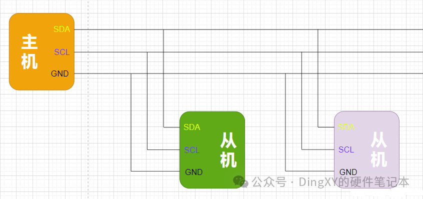
(2) The I2C bus is a multi-master bus, where devices connected to the I2C bus are classified as masters and slaves.
① The master has the authority to initiate and terminate a communication, while the slave can only respond to calls.
② When multiple masters are enabled on the bus simultaneously, I2C also has conflict detection and arbitration capabilities to prevent errors.
③ Each device connected to the I2C bus has a unique address (7 bits), and each device can act as both a master and a slave (but only one master can exist at a time). Adding or removing devices on the bus does not affect the normal operation of other devices.
④ During communication on the I2C bus, the device sending data is called the transmitter, and the device receiving data is called the receiver.
(3) The I2C bus can be online tested through external wiring, facilitating system fault diagnosis and debugging. Faults can be immediately addressed, and software can be standardized and modularized, reducing development time.
(4) The number of devices that can be connected to the I2C bus is limited by the maximum bus capacitance of 400pF, with practical design experience suggesting no more than 8 devices.
(5) The serial 8-bit bidirectional data transmission rate can reach 100Kbit/s in standard mode, 400Kbit/s in fast mode, and 3.4Mbit/s in high-speed mode.
(6) The bus has extremely low current consumption, strong anti-noise interference capability, and adding bus drivers can increase the bus capacitance by ten times, allowing transmission distances of up to 15m; it is compatible with devices of different voltage levels and has a wide operating temperature range.
1.2 I2C Bus Data Transmission Protocol
(1) Start Signal
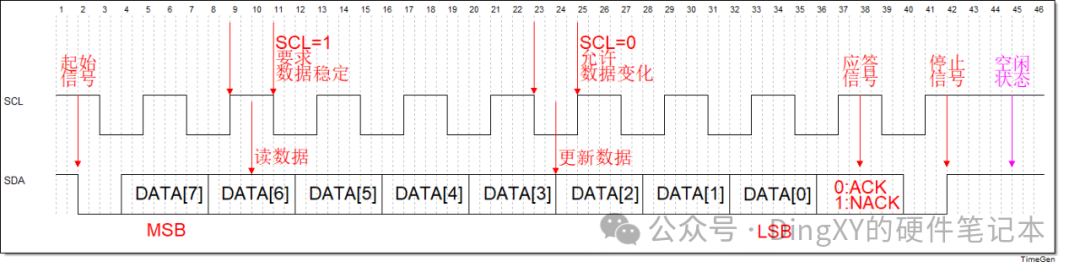
When SCL is high, a transition of SDA from high to low indicates a start signal, which is a level transition timing signal rather than a level signal. This signal is generated by the master, and once the start signal is generated, the bus is in a busy state, preparing for data transmission.
(2) Stop Signal
When SCL is high, a transition of SDA from low to high indicates a stop signal; this signal is also a level transition timing signal rather than a level signal. This signal is generated by the master, and once the stop signal is sent, the bus is in an idle state.
(3) Acknowledge Signal
After the transmitter sends a byte, it releases the data line during the 9th clock pulse, and the receiver sends back an acknowledge signal. When the acknowledge signal is low, it is defined as an acknowledge bit (ACK), indicating that the receiver has successfully received the byte; when the acknowledge signal is high, it is defined as a non-acknowledge bit (NACK), generally indicating that the receiver has not successfully received the byte.
(4) Data Validity
During data transmission on the I2C bus, the data on the data line must remain stable while the clock signal is high. Changes in the data line’s high or low state are only allowed when the clock line signal is low. Data must be prepared before the rising edge of SCL and must remain stable before the falling edge arrives.
(5) Data Transmission
Each bit of data transmitted on the I2C bus corresponds to a clock pulse (or synchronous control), meaning that under the coordination of the SCL serial clock, each bit of data is transmitted serially on the SDA line. The transmission of data bits is edge-triggered.
(6) Idle State
The I2C bus is considered to be in an idle state when both SDA and SCL lines are high. At this time, the output stage field-effect transistors of each device are in the cutoff state, releasing the bus, and the pull-up resistors on both signal lines pull the level high.
1.3 Clock Synchronization and Arbitration on the I2C Bus
(1) Clock Synchronization
The clock synchronization signal during information transmission on the I2C bus is completed by the logical “AND” of all devices connected to the SCL line. That is, if multiple masters generate clocks simultaneously, the SCL line will only show high when all masters send high; otherwise, SCL will show low.
A transition from high to low on the SCL line will affect these devices. Once a device’s clock signal drops to low, it will keep the SCL line low, causing all devices on the SCL line to enter a low period. At this time, devices with shorter low periods will not affect the state of the SCL line, and these devices will enter a high waiting state. When all devices’ clock signals rise to high, the low period ends, and the SCL line is released back to high, meaning all devices start their high period simultaneously. Subsequently, the first device to end its high period will pull the SCL line low, creating a synchronized clock on the SCL line.
Thus, the duration of the clock low period is determined by the device with the longest low period, while the duration of the clock high period is determined by the device with the shortest high period.
(2) Clock Arbitration
Bus arbitration is similar to clock synchronization; when all masters write 1 on SDA, the data on SDA is 1. If any master writes 0, then the data on SDA is 0.
Each time a master sends a bit of data while SCL is high, it checks whether the level of SDA matches the data being sent. If it does not match, the master knows it has lost arbitration and stops writing data to SDA. In other words, if a master consistently finds that the data on the bus matches the data it sent, it continues transmission, ensuring that the master that wins arbitration does not lose data during the arbitration process.
A master that loses arbitration will stop generating clock pulses after detecting it has lost and can only resume transmission when the bus is idle.
The arbitration process may involve multiple bits of sending and checking. In practice, if two masters send with exactly the same timing and data, both masters can successfully complete the entire data transmission.
1.4 Address Byte for I2C Slave Devices
(1) 7-bit Address for Slave Devices
Address Byte (1 Byte) = [7-bit Address + 1-bit Read/Write Control Bit (1: Read W, 0: Write R)]
(2) 10-bit Address for Slave Devices
Address Byte (2 Bytes) = [11110 + 2-bit Address 10th and 9th bits + 1-bit Read/Write Control Bit (1: Read W, 0: Write R)] + [8-bit Low 8 bits of Address]
(3) Other Considerations
① “11110xx” is one of the 16 special instruction addresses reserved in I2C communication, and only 10-bit address slave devices will respond to this address.
② In an I2C communication system, both 7-bit and 10-bit address slave devices can coexist and are compatible.
③ If the master device communicates continuously with a 10-bit address slave device, only the first byte needs to be transmitted during the second communication.
2. Implementation of I2C Bus Communication Process
2.1 I2C Bus Data Read/Write Flow
2.2 Definition of I2C Communication Process
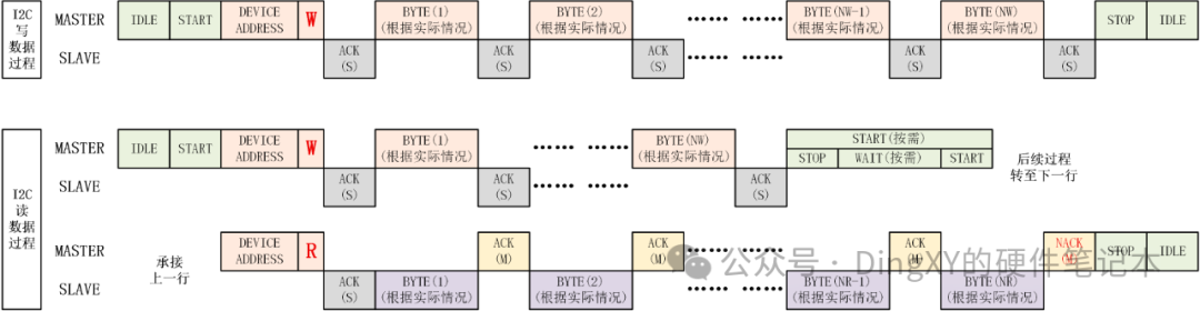
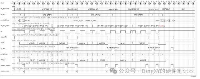
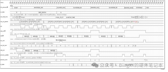
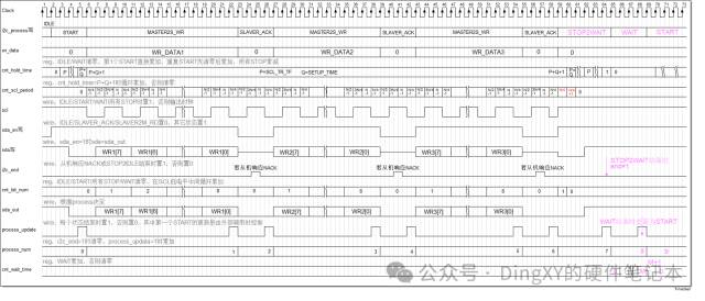
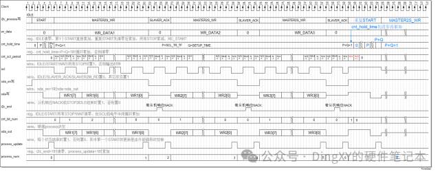
IDLE = 4'd0START = 4'd1MASTER2S_WR = 4'd2SLAVER_ACK = 4'd3SLAVER2M_RD = 4'd4MASTER_ACK = 4'd5MASTER_NACK = 4'd6WAIT = 4'd7STOP2IDLE = 4'd8STOP2WAIT = 4'd92.3 Fixed Combination Form of I2C Communication Process
Write DataIDLE--START--(MASTER2S_WR--SLAVER_ACK can repeat)--STOP2IDLE--IDLERead DataIDLE--START--(MASTER2S_WR--SLAVER_ACK can repeat) --(SLAVER2M_RD--MASTER_ACK can repeat) -- SLAVER2M_RD--MASTER_NACK --STOP2IDLE--IDLERead/Write WaitIDLE--START--(MASTER2S_WR--SLAVER_ACK can repeat)--STOP2WAIT--WAIT --START--(MASTER2S_WR--SLAVER_ACK can repeat) --(SLAVER2M_RD--MASTER_ACK can repeat) -- SLAVER2M_RD--MASTER_NACK --STOP2IDLE--IDLERead/Write ContinuousIDLE--START--(MASTER2S_WR--SLAVER_ACK can repeat) --START--(MASTER2S_WR--SLAVER_ACK can repeat) --(SLAVER2M_RD--MASTER_ACK can repeat) -- SLAVER2M_RD--MASTER_NACK --STOP2IDLE--IDLE3. Verilog Code (Private message “i2c_driver” to obtain)
3.1 Function Description
(1) General I2C Communication Function Module
(2) Can design the communication process based on actual conditions when called externally, with a maximum of 500 bytes read/write at a time
(3) External Call Considerations
① Design the complete I2C communication process based on process_update and process_num combined with the fixed combination form
② The process updates to (first) START are controlled by external calls
③ The process updates to MASTER2S_WR when updating wr_data
④ The process updates to SLAVER_ACK when wr_data needs to be cleared
⑤ The process updates to WAIT when updating wait_time
⑥ The process updates to (second) START when wait_time needs to be cleared
⑦ The process updates to MASTER_ACK or MASTER_NACK when obtaining rd_data
⑧ After the process STOP2IDLE ends, update the process to IDLE; after the process STOP2WAIT ends, update the process to WAIT
⑨ After the signal i2c_end is high, update the process to IDLE
3.2 Explanation of Simulation Process for Slave Device Data Line SDA
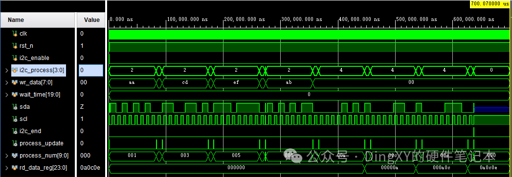
//---------------------------------------------------------------------------------------------// I2C Communication Data Line SDA (High Level When Idle)//---------------------------------------------------------------------------------------------/*【1】 Actual Applicationassign sda = (sda_en == 1'b1) ? sda_out : 1'bz ;//*///*【2】 For Simulation: Set the response data of the I2C slave to the low 8 bits of process_numassign sda = (sda_en == 1'b1) ? sda_out ://MASTER controls sda data line (i2c_process == SLAVER_ACK) ? 1'b0 : //Slave responds ACK (i2c_process == SLAVER2M_RD) ? process_num[8-cnt_bit_num] : 1'bz ;//*/3.3 Timing Diagrams
(1) Timing Diagram 1: Writing Data STOP2IDLE
(2) Timing Diagram 2: Reading Data STOP2IDLE
(3) Timing Diagram 3: Read/Write Wait STOP2WAIT
(4) Timing Diagram 4: Continuous Read/Write RE_START
3.4 Source Code
See code on CSDN account https://blog.csdn.net/sinat_36503471?type=blog3.5 TestBench Simulation Code (Read/Write Wait)
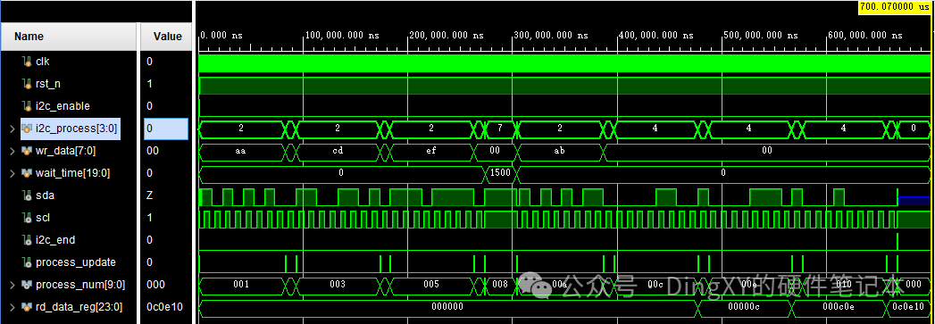
See code on CSDN account https://blog.csdn.net/sinat_36503471?type=blog3.6 Simulation Results (Read/Write Wait)
3.7 TestBench Simulation Code (Continuous Read/Write)
See code on CSDN account https://blog.csdn.net/sinat_36503471?type=blog3.8 Simulation Results (Continuous Read/Write)