The previous article introduced GTX transmitter, and this article will introduce GTX RX receiver. The structure of the GTX RX receiver is similar to that of the TX transmitter, with the data flow direction reversed. However, there are some differences from the transmitter. The structure diagram of the GTX RX receiver is shown in Figure 1:
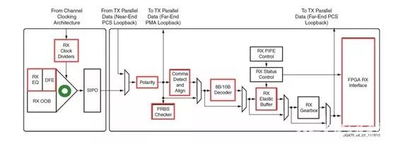
Figure 1
Below, we will introduce the functions of each circuit part of the RX receiver based on the data flow direction.
RX Equalizer (DFE and LPM):RX signals enter from AFE (Analog Front End) and first go through the RX equalizer. The main function of the equalizer is to compensate for high-frequency losses during signal transmission through the channel. Since the channel is bandwidth-limited, the signal will inevitably suffer from attenuation or even damage.
The RX receiver has two types of equalizers, namely LPM and DFE, which differ in power consumption and performance. The LPM has lower power consumption, while the DFE can provide more accurate filter parameters, thus compensating better for transmission channel losses, resulting in better performance.
RX CDR:The RX clock data recovery circuit is the green circle portion in Figure 1. Since GTX transmission does not carry a clock signal, the receiver must perform clock recovery and data recovery on its own. The clock data recovery circuit is shown in Figure 2:
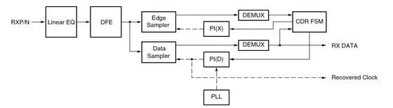
Figure 2
The specific process is shown in Figure 2. First, external data comes in and goes through the equalizer, and then the data output from the equalizer enters the clock data recovery circuit. GTX uses a phase-rotating CDR structure. Data coming from DFE is captured by both edge sampler and data sampler, and then the CDR state machine determines the phase of the data stream based on both and feeds back control to the phase interpolator ( PI). When the position of the data sampler is at the center of the eye diagram, the edge sampler locks onto the transmission domain of the data stream. The CPLL or QPLL provides the base clock for the phase interpolator, allowing the CDR state machine to perform phase control effectively.
RX Fabric Clock Output Control:The RX receiver’s clock structure is very similar to that of the TX transmitter, as shown in Figure 3. The red box part of the CDR in the figure is the biggest difference from the TX side.
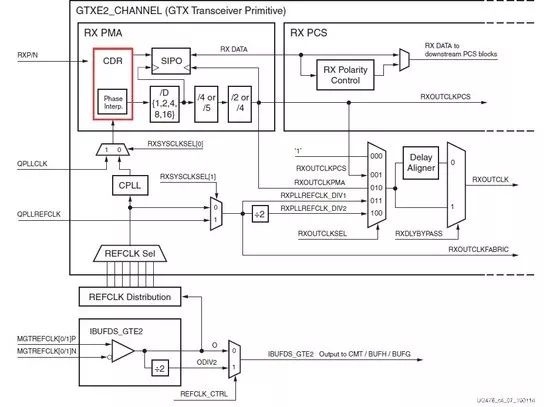
Figure 3
Similar to the TX transmitter, the RX receiver’s clock structure is mainly divided into serial clock divider and parallel clock divider. The D divider is the serial clock divider used to reduce the PLL clock rate to support lower line rates, while the parallel clock divider mainly generates different parallel data clocks based on the set bit width and whether to use 8b/10b.
RX Polarity Control:Like the TX transmitter, the RX receiver also has a polarity control function, which can be used to implement data flipping. This function is used when RXP and RXN are reversed during PCB design.
RX Pattern Checker:GTX includes an embedded PRBS checker, as shown in Figure 4. There are four different pseudo-random sequence generators to choose from, and the checker is self-synchronizing, working before boundary alignment and decoding. This function can be used to test the integrity of the signal.
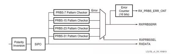
Figure 4
RX Byte and Word Alignment:Before serial data is parallelized, it needs to find an appropriate feature boundary. This feature boundary or character boundary is identified by a recognizable sequence sent by the TX transmitter, commonly referred to as an identifier ( comma) or K code. The receiver searches for this identifier in the incoming data, and once found, the subsequent received data is parallelized based on this identifier as the boundary. Its working principle is shown in Figure 5.
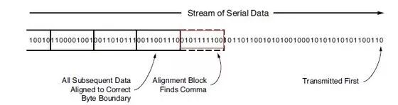
Figure 5
As shown in Figure 5, when the comma is found in the serial data (red box), the subsequent data is aligned based on this boundary.
RX 8B/10B Decoder:If the data sent by the transmitter is 8B/10B encoded, then the receiver needs to perform 8B/10B decoding; otherwise, it can be bypassed. This function was mentioned when introducing the TX transmitter and will not be described again here.
RX Elastic Buffer:The RX receiver elastic buffer is an important function. Compared to the TX receiver buffer, the RX has an “elastic” property, which means that the RX elastic buffer has more functions ( RX clock correction and RX channel bonding) compared to the TX transmitter. The RX elastic buffer’s position in the RX receiver is shown in the green box of Figure 6.
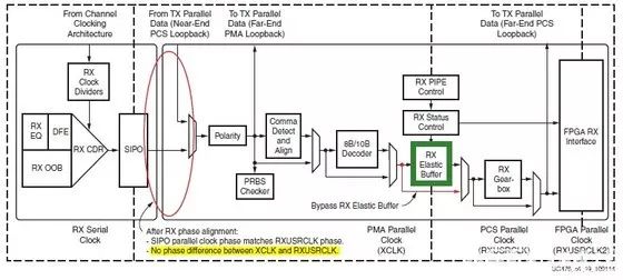
Figure 6
From Figure 6, it can be seen that the RX receiver PCS sub-layer mainly has two clock domains, namely XCLK and RXUSRCLK domains. The RX elastic buffer function is mainly used to match the phase difference between the two clocks.
If this RX elastic buffer is bypassed, certain conditions must be met to ensure stable data reception. First, a phase alignment circuit is needed to handle the phase difference between the SIPO circuit clock and XCLK clock. Secondly, XCLK needs to be configured to the RXUSRCLK clock to ensure that XCLK and RXUSRCLK are in the same clock domain without phase difference.
RX Clock Correction:The “elasticity” of the RX elastic buffer reflects the ability to adjust the frequency difference between XCLK and RXUSRCLK through clock correction. For the RX receiver, even if XCLK and RXUSRCLK run at the same clock frequency, there are often certain differences, which can easily lead to the RX elastic buffer being filled or emptied. The clock correction function is thus introduced. The clock correction function is shown in Figure 7.
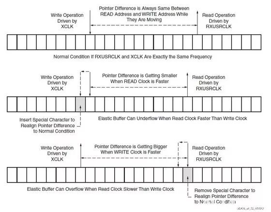
Figure 7
In simple terms, during the TX transmitter phase, we periodically send K codes to ensure that the receiver aligns boundaries. When data is insufficient in the RX elastic buffer, the received K code data will be copied into the RX elastic buffer to keep it half full. When the RX elastic buffer has too much data, the received K code data will be discarded and not written into the RX elastic buffer to keep it half full.
RX Channel Bonding:The channel bonding function also reflects the “elasticity” of the RX elastic buffer. For protocols like PCIE and SRIO, it can support multi lane transmission to improve total transmission bandwidth. Due to the nature of the transmission channel, the data sent by the TX transmitter at the same time cannot be received by all lanes at the same time. Each lane has a time difference in receiving, so when recovering data, it needs to be realigned. Therefore, the channel bonding function needs to be executed at the RX receiver.
To implement this function, the TX transmitter adds the same channel bonding sequence to the data stream. At the RX receiver, adjustments and delays are made in each RX elastic buffer based on the channel bonding sequence detected by each lane, ultimately ensuring that the data from each lane is aligned without offsets, as shown in the FPGA RX Interface output. The left side shows unaligned data, while the right side shows aligned data, as illustrated in Figure 8.
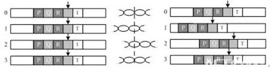
Figure 8
FPGA RX Interface:Users receive data through the FPGA RX Interface, similar to the TX transmitter. Data is received on the rising edge of RXUSRCLK2 (the TX transmitter sends data on the rising edge of TXUSRCLK2). This user port can be set to 16/20/32/40/64/80 bit widths, and the rate of RXUSRCLK2 is determined by the RX line rate, RXDATA bit width, and whether 8B/10B is enabled. The specific ports are shown in Table 1. Similar to the TX, it will not be described further.
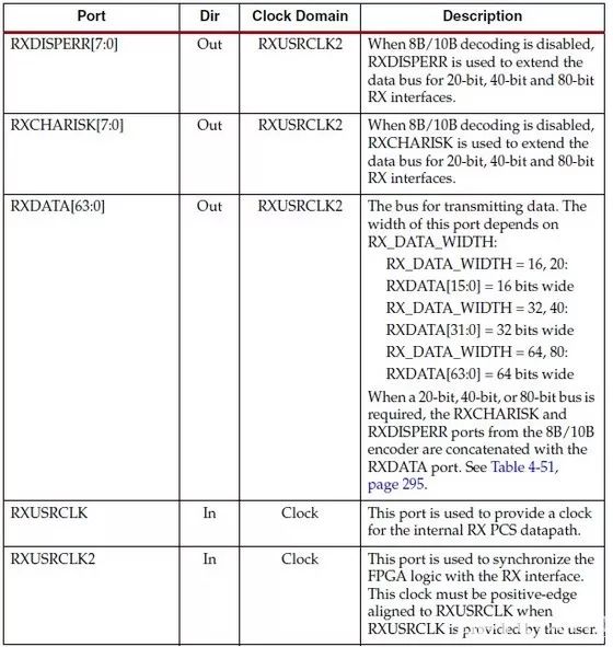
Table 1
This concludes the introduction of the RX receiver. The next blog will introduce how to use the 7-Series Transceivers IP.
Recruitment Information