Welcome FPGA engineers to join the official WeChat technical group.
During remote updates, sometimes dual images are needed to ensure the stability of the design. When updating the design, only one image is updated, while the other image has been tested and does not require updates before deployment. If an update fails, operations can be performed using the unupdated image to rewrite the failed data back to Flash. This way, even if the update fails, the design can still be remotely recovered.
Xilinx’s dual image solution is called Multiboot. This article provides a brief introduction to the Multiboot of Xilinx 7 series.
Multiboot directly operates on two images, but it can actually be used for multiple images. For convenience, the two images in Multiboot are referred to as the G image (Golden) and the M image (Multiboot).
For remote update solutions, some involve the FPGA reading and writing Flash, such as the Flash read/write controller that needs to be implemented on the Xilinx platform, and the ASML IP on the Altera platform. When other connections like JTAG cannot be provided, the only solution for Flash updates is through the FPGA.
When an error occurs during the Flash write operation, or if data in certain addresses in Flash becomes corrupted, it can lead to an unsuccessful FPGA load.
When the FPGA fails to load successfully or operates abnormally, the read/write operations on Flash cannot be guaranteed. At this point, it is also impossible to re-read and write Flash through the remote update solution to correct previous errors. Therefore, it can be seen that if Flash is directly controlled by the FPGA, errors during remote updates are likely to render the remote update completely ineffective, necessitating on-site updates for repair.
The corresponding solution is to use dual images (or multiple images), where only the M image is updated during the update process, and the M image is used directly after the update. If an error occurs during the M image update, the G image is activated. The design in the G image is then used to update the data in the M image portion of Flash.
Since the G image has never been updated, the probability of error is very low. Thus, even if the M image encounters an error, some operations (like Flash read/write operations) can still be completed through the G image, ensuring the design remains operational.
From this analysis, it can be concluded that the dual image solution requires the completion of two tasks.
1. Under normal circumstances, the M image should be running upon completion of loading.
2. In case of errors, it needs to revert to the G image.
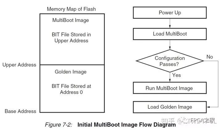
As shown in the figure above, the Multiboot solution for Xilinx 7 series FPGAs stores the G image starting from the base address, followed by the M image. During the loading process, the M image is loaded first; if successful, it runs the M image; if it fails, it reloads the G image.
Next, we will introduce the two tasks that need to be completed in conjunction with the above figure.
First, let’s look at the first task, loading the M image.
After powering on, the FPGA will perform loading operations according to the settings. In active mode, the FPGA will begin operations on the Flash, attempting to read the configuration image data stored in Flash. It is important to note that this series of operations in active mode is automatically completed by the FPGA, and the user cannot control it.
This leads to the first question. Since the read operation is automatic, how does the FPGA know where the M image is stored and load the M image first? If it starts reading from address 0, it should first complete loading the G image. Otherwise, how is the address for using Multiboot and the M image communicated to the FPGA to inform it?
The solution in Xilinx’s Multiboot scheme is to use a loading command: IPROG. This command is placed in the G image.
Specifically, for the FPGA to read directly from address 0, it starts loading the G image, but this G image is specially processed, with the IPROG command and the address of the M image added at the beginning of the image data. When the FPGA reads this command, it will skip the subsequent data and continue loading from the set address. This operation ensures that the G image only executes the initial loading commands, while the M image begins loading after only a few commands, guaranteeing direct loading of the M image.
It should be noted that IPROG is a command, so it can be effective both in the G image and in any design. Users can send the IPROG command to the ICAP to trigger reloading at any time. By setting appropriate addresses, multiple image switches can be achieved.
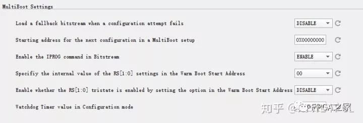
From the settings in Vivado, it can be seen that the main settings for Multiboot consist of these six items. The first is called Fallback, and the last is called Watchdog. These two will be introduced later. The fourth and fifth are about the RS pin. Once familiar with Multiboot, you can refer to the documentation for understanding; this article will not go into further details.
The second is to set the address to jump to, and the third is to add the IPROG command in the G image. These two operations can be sent to the ICAP interface in command form to trigger the jump and load new image data in Multiboot.
After reviewing the above analysis, you should understand how to fulfill the requirement of loading the M image first. The next step is to understand how to revert to the G image when loading fails.
If the M image fails to load, the operation to revert to the G image is referred to as Fallback in the Multiboot scheme.
Fallback will be triggered under four conditions:
1. ID Code error 2. CRC error 3. Watchdog timeout 4. BPI address overflow
ID Code error refers to a mismatch between the device model in the configuration file and the current device. CRC check means that after the configuration data is sent to the FPGA, it will be checked, and if the data is different, a CRC error will be indicated. These two basic principles are relatively easy to understand; for specific details, one must be able to parse the contents of the bit file to fully understand.
Watchdog timeout means that if the configuration is not successful within a specified time, it triggers a Watchdog timeout, which will lead to Fallback.
BPI address overflow refers to the gradual increase of the BPI address exceeding the maximum value, causing an overflow and reverting to 0, thus triggering Fallback.
After roughly understanding the four conditions, it can be seen that BPI is only applicable to BPI mode, and is somewhat similar to Watchdog, where if loading is not successful within a certain period, the address gradually increases, and the timer increases, exceeding the range will trigger Fallback, so no further explanation will be provided for BPI.
ID Code also does not require further explanation, as an incorrect ID Code likely means the wrong image file was used, so there isn’t much to analyze.
The key point is 2 and 3. When there is a Multiboot image, if there is an issue with the content of the M image, it will trigger a CRC check error, ensuring that the image loads successfully and the data is correct.
However, if there is no Multiboot image, the CRC check cannot be performed, or it hangs halfway through loading. At this point, the Watchdog needs to trigger Fallback. As long as the loading is not completed within a certain time, the Watchdog timeout will definitely be triggered.
Therefore, CRC is used to ensure correct loading, while Watchdog is used to ensure that loading failure is reported.
Note that the timing settings for the Watchdog should be set appropriately and tested in practice, rather than relying solely on experience/documentation to infer an appropriate value.
After a Fallback occurs, the project will revert to address 0 and begin loading the G image. Here, the FPGA’s internal configuration registers will record the state during the loading process. When a Fallback occurs, it will automatically ignore the IPROG command and directly load the subsequent parts of the G image, ensuring that the G image has the opportunity to be fully loaded.
The FPGA has some built-in registers that record certain states during FPGA loading, commonly referred to as the device status registers. When loading fails, relevant registers can be checked via JTAG to find clues to help locate the problem.
Through this series of complex operations, dual image configuration switching can be achieved. The greatest advantage of this method is speed. After configuration is complete, it allows for quick jumps, loads, and returns. The key point is that the dual image selection occurs right at the beginning of the loading process, making the jump very rapid, suitable for scenarios that require strict configuration times. The downside is that the principles and settings are relatively complicated.
In contrast to the above method, another method for dual image switching is for users to perform the switching themselves. The general principle is that users utilize the FPGA’s programmable logic resources to control the ICAP module, input the desired jump address, and then input the IPROG command to trigger the jump operation. This operation requires the G image to be loaded and running first, then the user controls when to perform the jump.
The advantages of this operation include:
1. The jump address is chosen by the user, allowing for switching among multiple images, not limited to two;
2. The user can choose to load at the right time, providing greater flexibility.
The main disadvantages are:
1. Requires a better understanding of the configuration process, ICAP port, and control commands;
2. Requires at least one image to be loaded before use, making it unsuitable for scenarios with high configuration time requirements.
If the goal is solely remote updates, then this solution is not suitable. The automatic dual image solution is simpler and easier to use. As long as the G image is debugged, the entire scheme has lower requirements for the M image.

Welcome communication engineers and FPGA engineers to follow our public account.

FPGA WeChat technical group
Everyone is welcome to join the national FPGA WeChat technical group, where there is a group of engineers who love technology, and you can discuss and exchange technology together!

Press and hold to join the national FPGA technical group.
FPGA IP core services: Various high-quality IP core service providers, with reliable service and guarantees! If you have needs, you can directly contact the group owner!
Self-operated FPGA technical group platform:XilinxAltera, Micron, Samsung, Hynix, ADI, TI, ST, NXP and other brand advantages distributors, everyone is welcome to send a model list whenever needed, and we will provide you with the most competitive quotes as soon as possible!Prices are more than 5% lower than your original supplier! Welcome to inquire – just send your needs to the group owner!
Official thanks to brands in the FPGA technical group: Xilinx, Intel (Altera), Microsemi (Actel), Lattice, Vantis, Quicklogic, Lucent, etc.