Xilinx 7 Series FPGA Built-in ADC
The entire Xilinx 7 series FPGA is equipped with an ADC, referred to as XADC. This XADC consists of two internal 1 Mbps ADCs that can convert analog signals into digital signals for internal FPGA use.
The XADC can directly obtain the chip junction temperature and several power supply voltages of the FPGA (the 7 series does not include VCCO) for monitoring the internal status of the FPGA. It also provides 17 pairs of differential pins, with one pair dedicated to analog differential input and 16 pairs multiplexed as analog differential inputs, which can be used as regular User I/O when not in use.
01
Pinout Requirements
XADC Pinout Requirements module pin requirements:
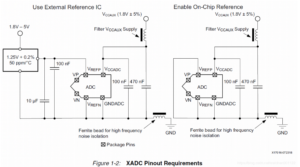
All dedicated pins for the XADC module belong to Bank0, hence the suffix _0 is added. The above figure 1-2 illustrates the basic input and output requirements of the XADC: there are two configuration requirements above, the left side uses Vccaux (1.8V) for power supply and an external 1.25V reference source. Using an external reference source can achieve better performance in terms of accuracy and thermal drift, and a ferrite bead is used to isolate the analog ground from the digital ground to avoid noise from common ground affecting the analog circuit; the right side uses the internal reference source, at this time, the VREFP pin must be connected to ground as shown. The table below lists the pin information for the XADC Package:
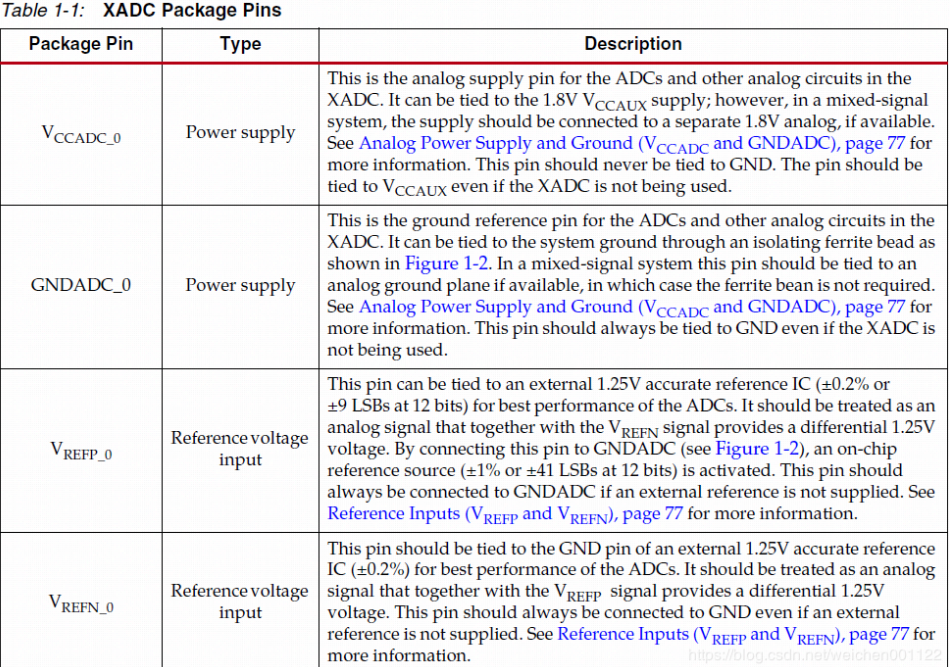
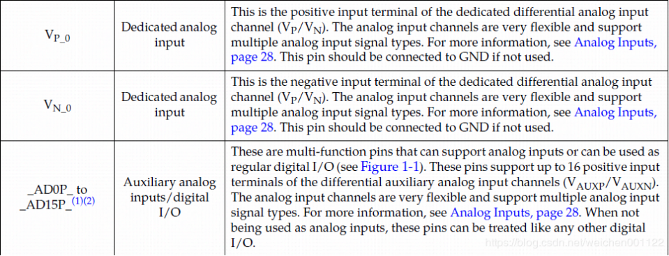
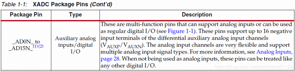
Note: The XADC module has a dedicated analog channel input pin (VP/VN) that supports differential input, and additionally up to 16 auxiliary analog channel input pins (ADxP or ADxN, where x ranges from 0 to 15). Kintex-7 does not support auxiliary channels 6, 7, 13, 14, and 15. Zynq-7000 AP SoC devices may not support all auxiliary channels due to different packaging, and specific packaging files should be consulted.
02
XADC Module Operating Modes
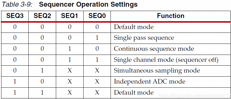
In single-channel mode, the user must select a channel to sample by writing to bits CH4 to CH0 of control register 40H. Additionally, the parameters BU (analog input mode) and ACQ (settling time) in control register 40H must also be set.
In independent ADC mode, ADC A is fixed to implement a default “monitoring mode,” where the alarm output function is enabled, and the user must set the correct alarm threshold; ADC B can only be used to measure external analog inputs.
In Single Pass mode, the ADC samples in the order specified by the user and stops after one complete sequence. The sampling order sequence is set by the user writing to the sequence channel selection registers 48H and 49H.
In Continuous Sequence mode, this mode is similar to Single Pass mode, except that after one complete sampling sequence, the system automatically restarts the sequence sampling, hence continuous sampling.
The mode selection is determined by bits SEQ3 to SEQ0 in control register 41H, as illustrated in the following figure:
03
IP Core Configuration
Basic Settings
Regarding the specific structure, function, and meaning of various parameters of the XADC, it is important to note:
1. The setting of the reference voltage will affect the error range and the calculation formula for the sampled value.
2. The analog differential input has requirements on the amplitude of the analog signal and requires some degree of conversion from the external analog circuit.
Assuming you need to use the XADC to obtain information from several analog signals, how should you proceed? The following explains one configuration method.
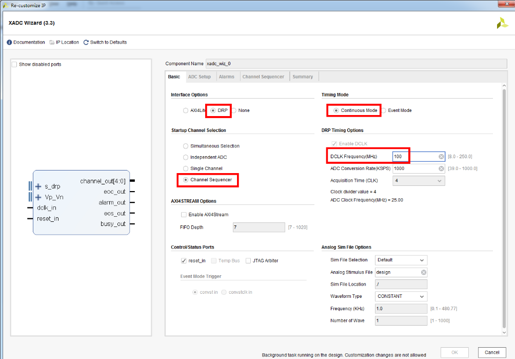
Pay attention to the points in the red box:
1. Use the DRP port to obtain digital signals, as this control seems simpler.
2. Use continuous sampling mode, where the ADC continuously operates in data acquisition mode and can output after sampling.
3. Use the Channel Sequencer mode; since there are only two XADCs and the data to be sampled is excessive, let the XADCs sample in sequence.
4. Set the clock frequency for the DRP port, either 50 or 100M is acceptable, with no special requirements.
ADC Setup Settings
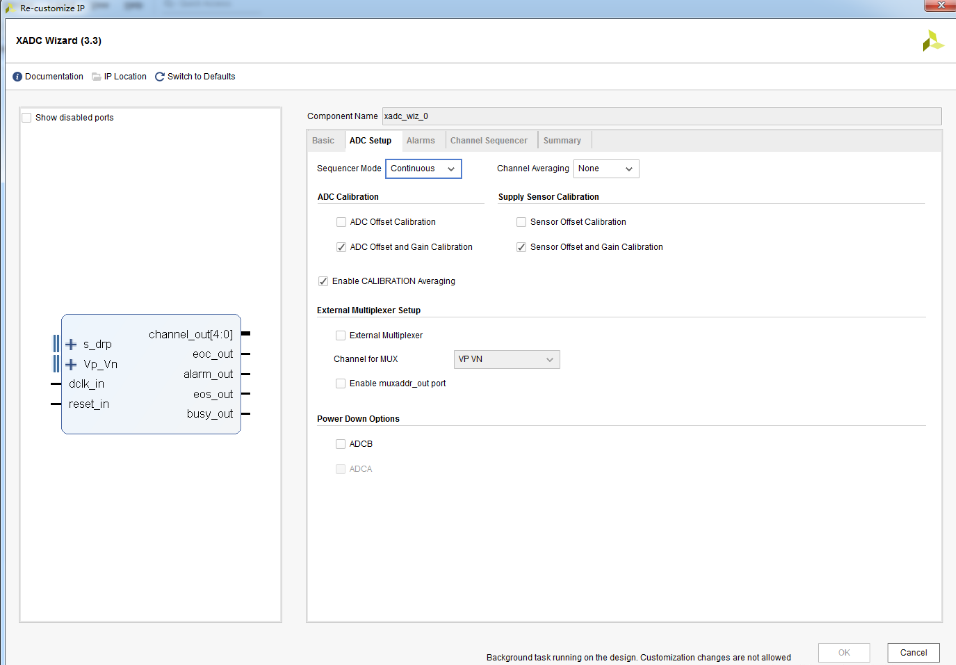
The second page of IP settings mainly sets Calibration, averaging, and external MUX. These can be temporarily skipped and explored later after becoming familiar with the use of XADC.
Alarms Settings
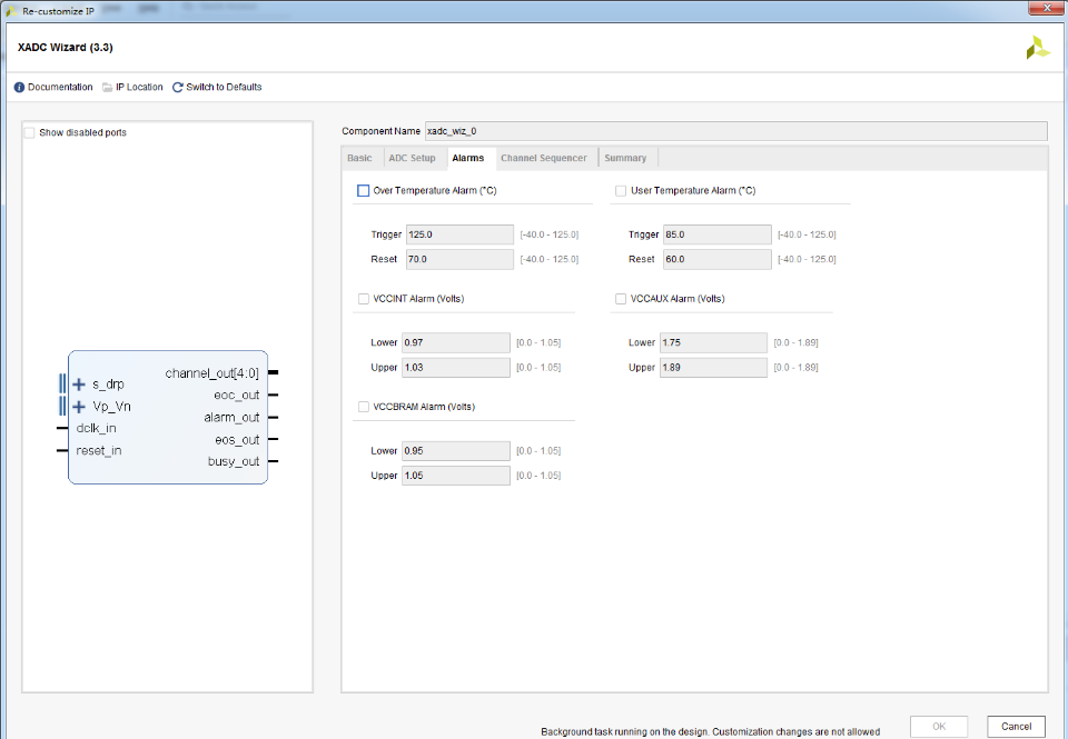
The third page sets alarm parameters, which can be left unset. If needed, you can set them for convenience.
channel Settings
The fourth page sets the channels to be used; here, select temperature and three power supply voltages, and choose one dedicated analog input channel and the first three multiplexed analog input channels.
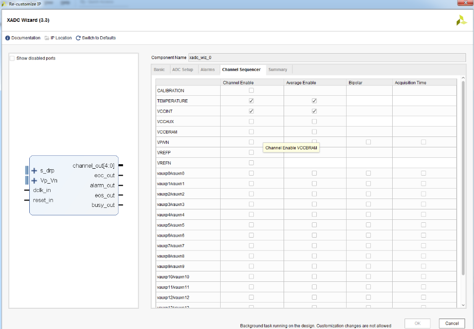
The final page is a Summary, where you can check if there are any issues with the settings and ensure there are no places that need adjustment.
At this point, the basic multi-channel data acquisition XADC is set up. As for areas not elaborated in the settings, you can research them after becoming proficient to find the most suitable usage mode.
04
Port Instantiation
Below is how to use this generated IP. Since the DRP port is used to read data, a DRP read-write controller needs to be designed. However, as the XADC itself provides some signals, this design is actually very simple.
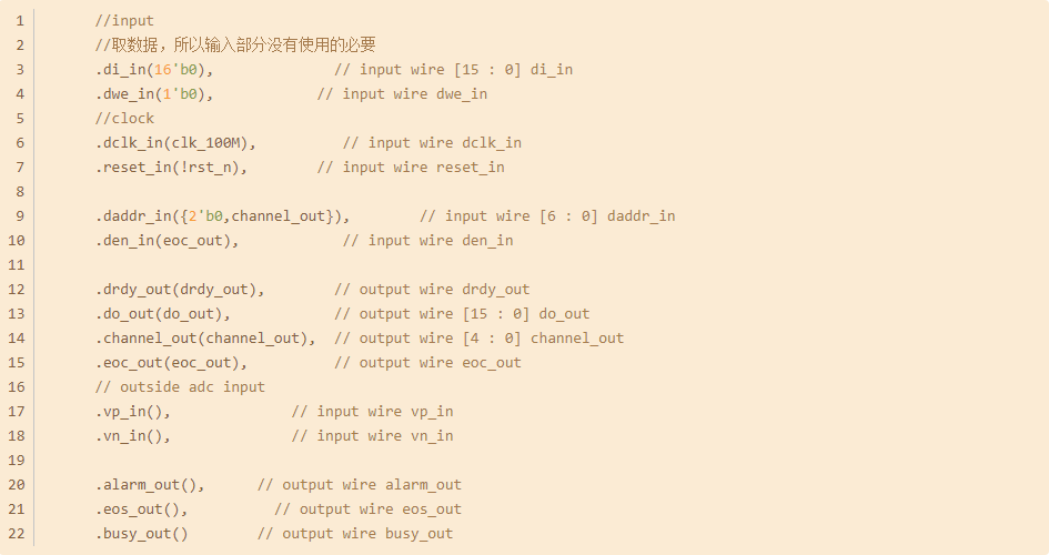
The remaining four DRP ports consist of two outputs and two inputs. The two outputs are directly exposed, where do_out is the final data needed. This port is 16 bits wide, and only the high 12 bits are required (corresponding to the 12-bit claimed in the XADC).
The XADC’s IP ports also include two named eoc_out and channel_out. Connect eoc_out to the den_in port of the DRP port, meaning that when sampling is completed for one of the multiple sampled channels, the DRP port operation is initiated to start reading data. After padding two bits to channel_out, send it to daddr_in as the address signal for DRP port operation. This completes the read-write operation of the DRP.
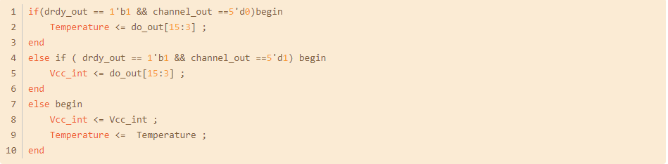
However, the output data will periodically change between several port data. Therefore, it is common to add a filtering setup at the backend, where the specific behavior is that when drdy_out, which indicates DRP operation completion, goes high, it uses the value of channel_out to determine which channel it is.
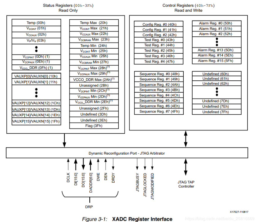
For the specific addresses of each sampling channel, please refer to the manual:
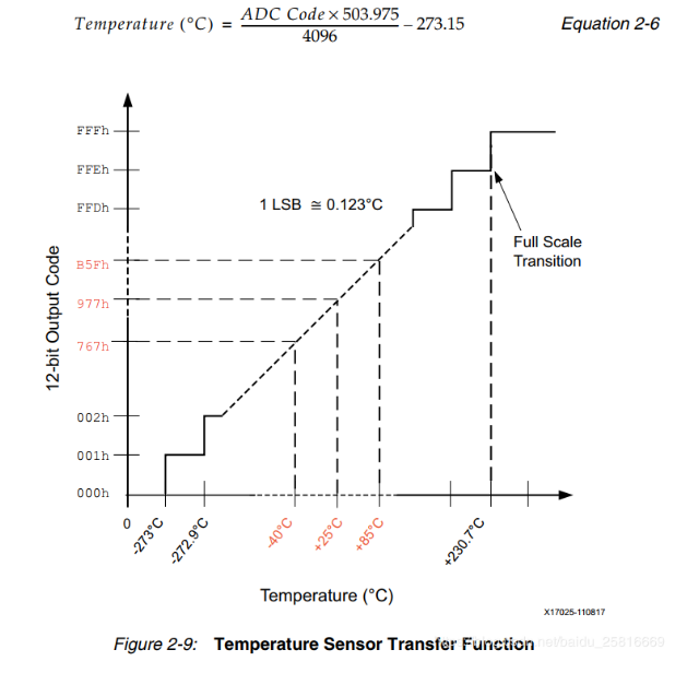
The temperature conversion formula and curve are shown in the following figure:
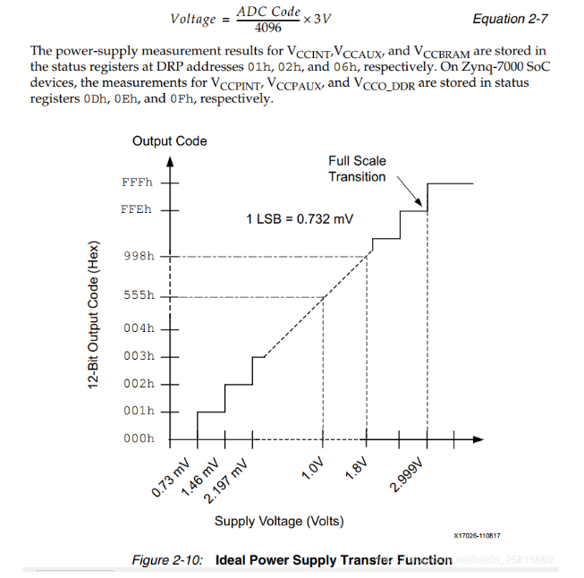
The voltage conversion formula and variation curve are shown in the following figure:
As for the analog differential input pins, they can be directly sent to the corresponding pins at the top level. Note that the Vivado tool may require level constraints for the multiplexed analog pins, selecting the appropriate lvcmos based on the voltage value of VCCO, for example, choosing lvcmos18 for a VCCO of 1.8V.
This way, the corresponding analog sampling data can be obtained. Since the analog signal changes that need to be detected are relatively slow in most cases, using XADC is sufficient for detection.
Issues related to the use of XADC also involve the MIG IP. MIG stands for Memory Interface IP, which is for DDR3 and similar DDR memory IPs. Since such interfaces generally operate at high speeds, temperature information is needed to make certain corrections to the interface. In the configuration of MIG IP, XADC is enabled by default.

At this time, the XADC only needs to provide temperature information. When more information is required, the XADC needs to be configured independently, which will generate two XADCs in the project; or instantiate two MIG IPs, each requiring one XADC. Since there is only one XADC module in the hardware, when the project needs multiple XADC modules, the tool will prompt an error.
The solution is also very simple: remove the XADC from the MIG IP. Then independently instantiate the XADC IP in the design. After obtaining the temperature information as described above, send it to MIG. After removing the XADC from the MIG IP, a temperature port will be generated to receive data, thus avoiding conflicts.
Another very convenient method to obtain temperature information is to use the Hardware Manager. By opening XADC in the Hardware Manager, you can see the temperature information.
In fact, all channel data of the XADC can be obtained through this method.
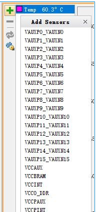
As seen in the above interface, the temperature information is Temp 60.3℃.