Flexible circuit board design has many advantages, but it also faces new design challenges.
Unlike “standard” 2D circuit boards, PCB design engineers encounter specific issues when designing flexible circuit boards. Understanding the characteristics of flexible circuit board design helps to address issues in advance and speeds up the design cycle.
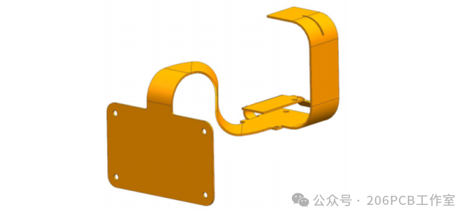
What is flexible circuit board design?
Almost all electronic devices require PCBs to function properly. However, with advancements in technology, the demand for smaller packaging and weight limitations have made flexible circuit boards increasingly common in design. This method pairs conductors with flexible insulating films, allowing them to carry the signals required for operation while maintaining flexibility: their ability to bend and flex means they can be used not only in electronic devices but also in mechanical applications. This approach was initially applied in space projects to save weight and space during missions and quickly found applications in military and consumer fields.
How to Choose the Right Type Based on Application
Currently, there are two types of flexible circuits: flexible circuit boards and rigid-flex circuit boards.
The former can mount devices on flexible plastic substrates, while the latter is a combination of flexible and rigid circuits. The rigid-flex design combines the advantages of both: the rigid board supports most components, while the flexible part connects them.
In recent years, with the increasing demand for smaller and higher-performance electronic products, the trend for flexible and rigid-flex designs has grown exponentially; smartphones and tablets are good examples. Flexible circuit board design is also making inroads into many other high-end consumer electronics, with limitless prospects.
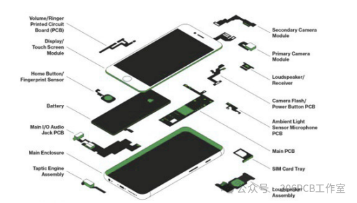
Flexible circuits have two usage types: static and dynamic.
Static flexible circuits are used with minimal bending frequency, typically during use and assembly.
Dynamic circuits are used in terminal systems that frequently bend, such as laptop hinges or printer heads. Distinguishing the final use of products is crucial to ensuring the appropriate materials and stacking methods are used to construct the circuits.
Wise Material Selection
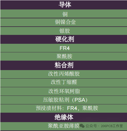
Building a flexible circuit involves a variety of materials.
These materials include films, copper foil, and adhesives. More commonly, polyester and polyimide are used, and the choice of material depends on how the circuit is assembled and used. Some materials may have additional advantages or disadvantages depending on our specific design intentions. When building flexible circuits, careful consideration of material selection is essential, and consulting manufacturers can help achieve the best possible decisions.
Design Considerations
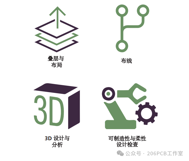
When designing a rigid-flex PCB, many critical design elements must be considered.
Each design topic is prone to serious accidents, so our choices are very important. Typically, projects have been underway for a long time before significant errors are discovered, forcing teams to backtrack and rework issues. Therefore, flexible, user-friendly, and feature-rich tools are necessary to meet our needs, helping us quickly identify problems in complex designs and guide us toward successful design paths.
Stacking
Flexible stacking configurations come in various forms, each with its own functionality.
Single-layer circuits are mounted on a single conductor layer made of metal or conductive polymers, covered by a flexible dielectric film. Single-layer circuits are currently the most commonly used and lowest cost circuit type. The structure of single-layer circuits is thin, functioning best in situations requiring constant movement.
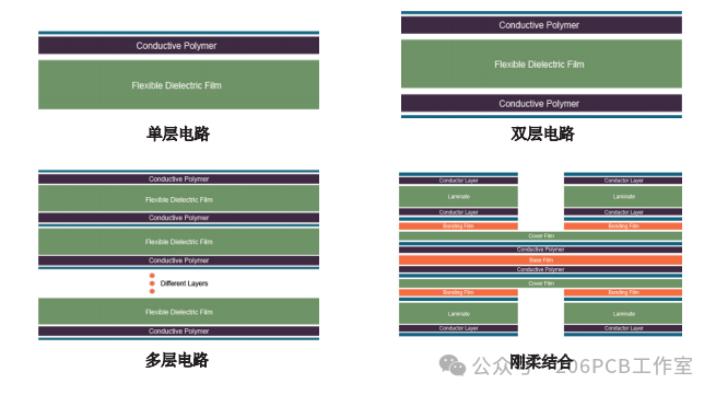
Double-layer circuits are placed on two conductor layers, with the main advantage being the ability to mount components on both sides of the circuit board. Use this type when shielding applications are critical to the design.
Multi-layer circuits span three or more layers, which may not be continuously bonded throughout the structure and may have openings or cavities. This type is more common in densely packed circuit installations.
Rigid-flex structures are a combination of flexible circuits placed on rigid and flexible substrates. They are then laminated into a single structure, making them an ideal choice for applications requiring stability and flexibility.
Layout
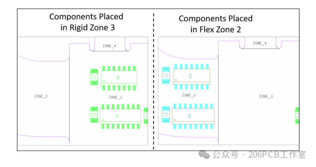
Different layout requirements exist for the flexible and rigid areas of circuit boards, which is unique to flexible circuit board design.
Smart component layout is the ability to place components in rigid or flexible areas and automatically position them in the highest component layer of that area. In both flexible states, we also need to check the gaps between z-axis components.
Bending Areas and Layer Structures
Bending areas require special consideration, especially along the bending lines of flexible circuits. To reduce stress, traces need to pass through bending areas that are perpendicular to the bending lines. Traces on adjacent layers should be offset to avoid forming I-beams. Designers must be able to set surface constraints and overlap constraints between objects on different layers. For example, pins and vias should not be in or near bending areas to prevent cracking.
Layer structures (also known as cross-sections) are set according to design requirements. In rigid-flex designs, not all areas of the circuit board contain all layers. Typically, the wiring layers in flexible areas are fewer than in rigid areas. We must ensure to avoid wiring in areas where layers do not actually exist.
Wiring
Flexible circuits face a series of unique challenges during wiring.
The bending capability of the circuit means it has specific design requirements. Wiring considerations and functional requirements include: arc corner wiring, sliding functionality for arc editing, and the ability to convert corners into arcs. Below is a brief overview of these wiring strategies, their usage timing, and their importance to flexible circuit board design.
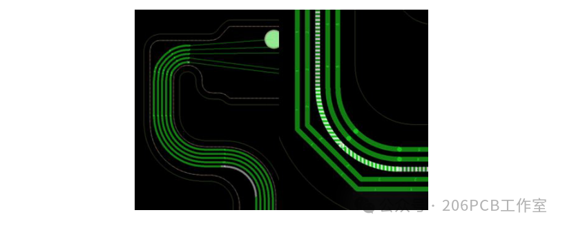
Arc corner wiring is the ability to wire traces with curved angles instead of orthogonal (45°) angles. Flexible circuit board design requires the use of curved traces to wire bus lines to reduce stress, so we must use arcs for wiring.
Pads have specific requirements to ensure robustness and longevity during use.
All pads, including surface mounts and through-holes, should be secured to prevent copper from separating from the substrate material. All pads should also have rounded corners to reduce stress points and eliminate fractures during bending. The quality of these components will determine the longevity of the end-user product, so careful inspection is necessary.
3D Inspection, Bending, and Flexing
Essentially, flexible circuit board design adds a layer of physical complexity.
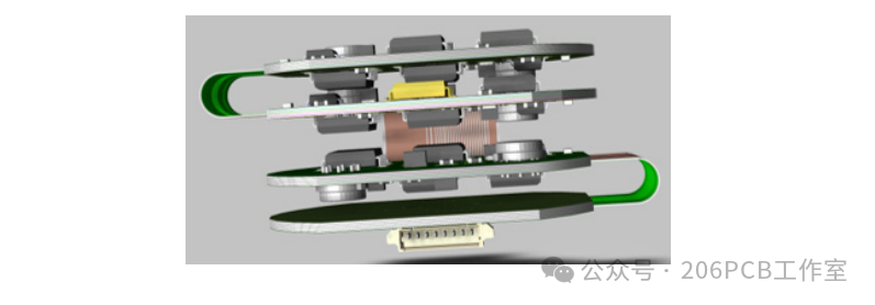
The complexity lies in the process of inspecting the final bent state of the circuit. All components must be precisely laid out to avoid collisions or interference in any bent areas. Therefore, design tools that can analyze the fit and gaps of bent circuits in a three-dimensional state are essential. Ideally, the analysis can be performed by the designer and should ideally be conducted in two stages: during the bending completion state and after the completion state. This helps identify issues in both states and alerts us to problems that arise between these two states.
Manufacturability Considerations
Flexible circuit board design requires unique manufacturability rules and inspections, as well as additional attention during manufacturer delivery.
Flexible circuit board design requires additional constraint checks to inspect gaps between objects on different layers. At this stage, maintaining clear communication with our manufacturers is crucial to understanding their specific constraints and allowances when building physical products.
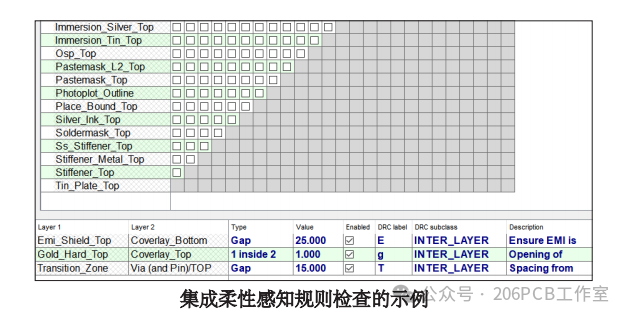
When conditions allow, the connection areas of flexible circuits should use mesh copper foils to reduce weight, enhance circuit flexibility, and prevent tearing. During the design process, using interlayer rule checks can timely identify errors, rather than discovering them too late and wasting valuable time. These rules are even more critical for multilayer dense circuit boards as they are more prone to various design errors. The distances between bending areas to reinforcement ribs, pads, and vias, as well as from coverings to pads, must be tracked. Using intelligent exchange formats (such as IPC-2581) allows manufacturers to more accurately capture our design intentions. Communicating with manufacturers early in the design cycle can provide us with the best possible feedback.