★ What is an “Annular Ring”? First, to understand “annular ring-free”, we need to know what an “annular ring” is. In traditional PTH (Plated Through Hole) design, a hole consists of three parts: ✒︎ Drill Hole: The hole drilled in the PCB. ✒︎ Copper Layer on Hole Wall: The copper layer formed on the hole wall through chemical deposition, used to connect different layers. ✒︎ Pad: The copper ring surrounding the hole on each layer. ♡♡ The part of the pad that is removed from the hole is what we refer to as the “annular ring”.
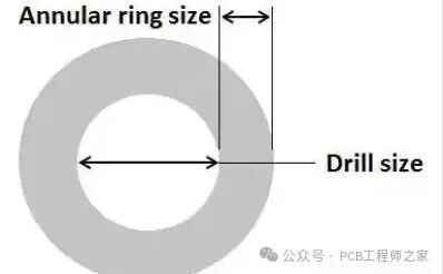
★ What is the function of the annular ring? ✒︎ Provides mechanical anchoring points
Ensures that the copper layer on the hole wall is firmly bonded to the copper foil of each layer, preventing detachment under thermal or mechanical stress. ✒︎ Ensures electrical connection reliability
Provides tolerance for alignment deviations during drilling, ensuring that even if the drilling is slightly off, it can still connect to the copper foil of that layer. ★ Why go “annular ring-free”? ✒︎ Difficulties in BGA Routing
Under fine-pitch BGAs, the space between pins is extremely limited. Traditional through holes with pads occupy a lot of space, making it impossible to route signal lines out from between the pins. ✒︎ Blocked Routing Channels
Pads can obstruct routing paths. If the pad is removed, routing can pass closely along the edge of the hole, greatly increasing routing flexibility and the number of available channels.
✒︎ Considerations for Mechanical Insulation
Sometimes components have metal housings or are metallic. If the annular ring is exposed, it may contact the component during assembly, leading to short circuits. Therefore, designing the hole as annular ring-free avoids short circuit issues. ♡♡ “Annular Ring-Free PTH” is essentially a design trade-off of “exchanging reliability for routing space”, creating pathways for signal lines by removing pads on non-critical layers.★ How is annular ring-free PTH achieved? “Annular ring-free” does not usually mean that the entire hole has no pads on all layers, but rather that pads are canceled (or made very small) on specific layers that do not need to connect to that hole. Common implementation methods include:
✒︎Direct annular ring-free or directly designing pads without holes, which is a relatively straightforward and typical design for annular ring-free holes. ✒︎ Hole in Pad + Plug Hole Plating A through hole is designed at the center of the BGA pad. The BGA pad itself acts as the “ring” for this hole, so this hole is “ringed” on the surface. However, this through hole will subsequently be filled with resin and plated flat to prevent solder from seeping in during soldering, resulting in a final product that appears