
Most engineers send the PCB files or Gerber files to the manufacturer and then wait for the boards to be returned. However, many hardware development professionals may work for years without the opportunity to visit a PCB manufacturing facility to see the entire production process.
Today, I will take you on a tour to see the complete process. (Source: Why Hardware?)
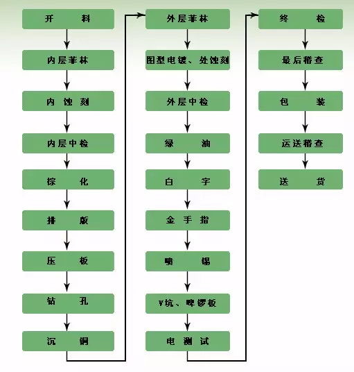
Step 1: Material Preparation
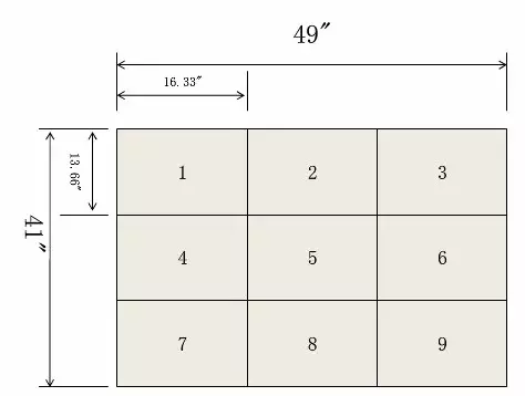
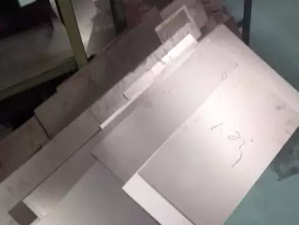
The raw materials for PCB manufacturing are generally in sizes of 1020mm×1020mm and 1020mm×1220mm. If the dimensions of the single board or panel do not fit well, a lot of raw material waste will be generated during the PCB production process. The PCB manufacturer will add the cost of this waste to your board, making the unit price of your PCB higher. If the board size is well designed, and the dimensions of the single board or panel are equal divisions of the raw material, then the utilization rate of the raw material will be maximized, allowing the PCB manufacturer to cut the material efficiently and produce the most boards from the same raw material size, resulting in the lowest unit price for the single board.
We cut the purchased copper-clad laminate into the required sizes, which is called material preparation.
Cutting Equipment: (Cutting large boards into smaller boards)
The earliest copper-clad laminates consist of a dielectric layer with copper laminated on both sides.
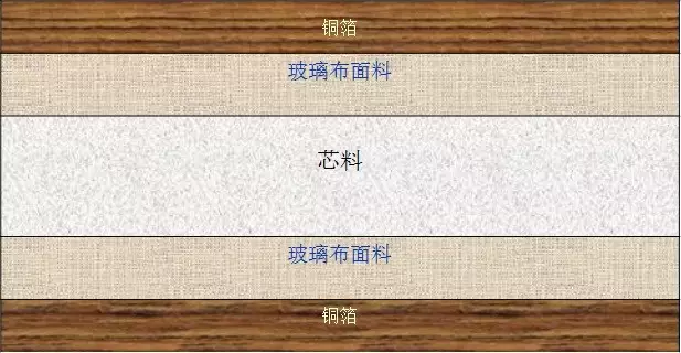
The above image shows a cross-section of a copper-clad laminate.
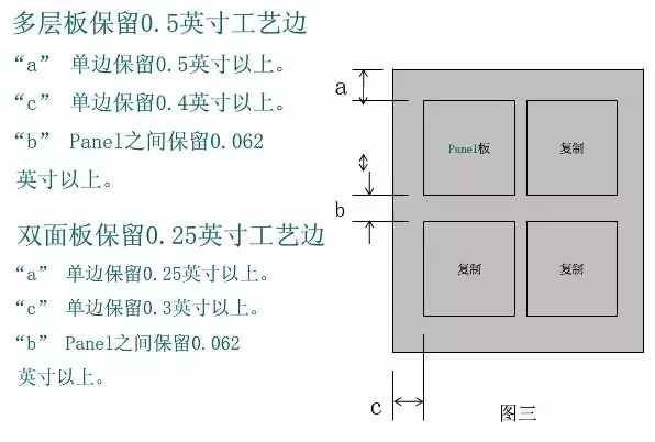
Step 2: Layout
Step 3: Film Generation
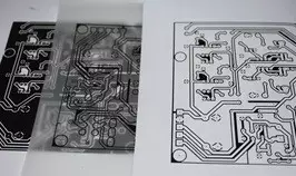
The graphic files provided by the customer are imported and modified using software, and the final graphics are output onto film. This means converting the Gerber files you provided to the manufacturer into film.
Film refers to a silver halide photosensitive film, also known as film. It is made from PC/PP/PET/PVC materials. Nowadays, it generally refers to photographic film, but it can also refer to the negatives used in printing. The film is always black.
Step 4: Exposure
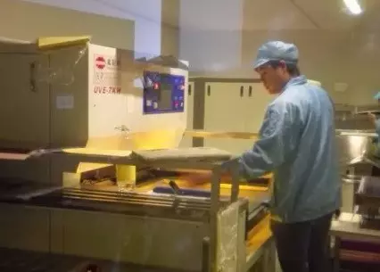
A layer of photosensitive liquid is coated on the surface of the copper-clad laminate, dried at 80 degrees Celsius, and then the film is placed on the PCB and exposed using a UV exposure machine, after which the film is removed.
The image below shows the exposure machine:
Step 5: Etching
The etching process can be broken down into the following steps:
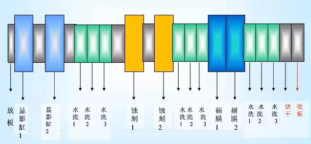
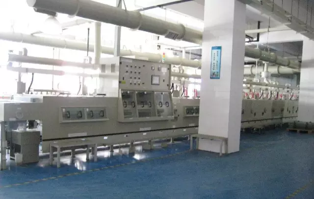
PCB etching machine
The board flows under the rollers
Why are the etching methods for inner and outer layers of PCB different?
Inner layer: Development → Etching → Stripping
Outer layer: Development → Copper plating → Stripping → Etching → Stripping
Why is this done? Isn’t the outer layer etching process more complicated?
The inner layer generally has larger line widths and spacing, so the ring is sufficient; the outer layer generally has denser lines and insufficient space, so at this point, we need to find a way to achieve the purpose of making the lines within the limited space. Alkaline etching can achieve a ring of 1-2 mils, but acid etching requires about 5 mils, so it is necessary to use tin to protect the required lines. Wherever possible, avoid alkaline etching because it is more expensive than acid etching. The etching factor is a factory’s manufacturing capability and cannot be improved through processes. The etching capabilities of acid and alkaline etching are simply different.
Step 6: Drilling
The machine drills holes in the PCB according to the sizes and coordinates specified in the files.
For non-metallic holes, the PCB factory must use dry film or perform secondary drilling or fill with glue, which will increase the cost for the factory. Therefore, if you do not specify, the factory will generally make metallized holes for you.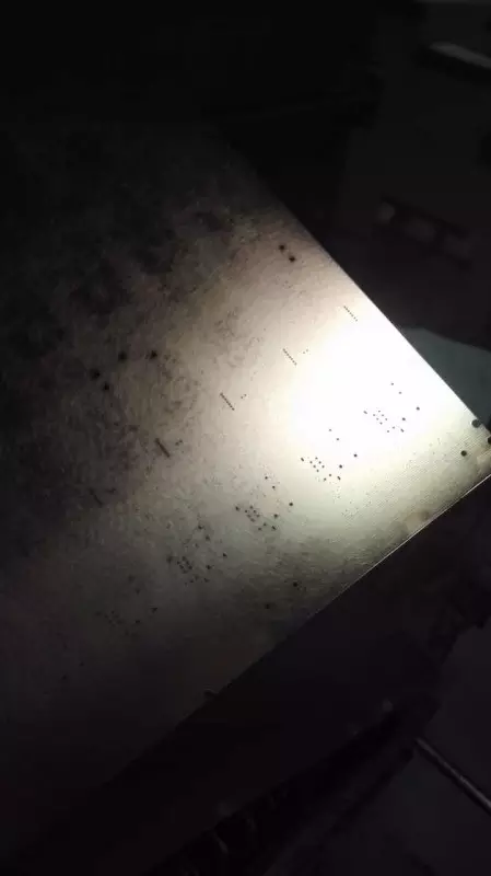
Step 7: Copper Plating
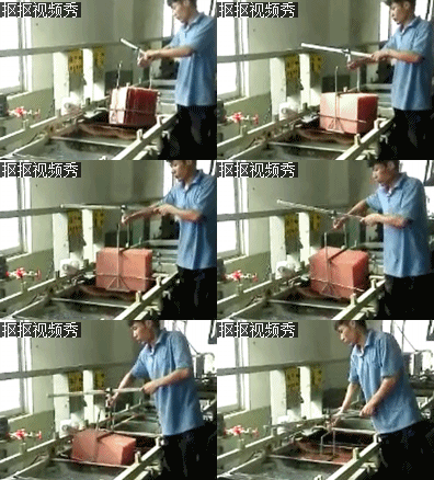
Copper plating is the process of depositing a layer of chemical copper on the non-conductive substrate (hole walls) and copper surfaces.
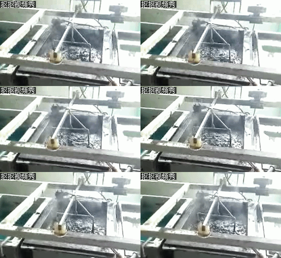
Step 8: Green Oil and Characters
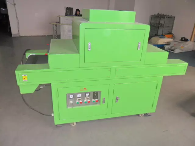
PCB Low-Temperature UV Machine, Purpose: Ultraviolet (UV) Coating Curing
Character Printing:
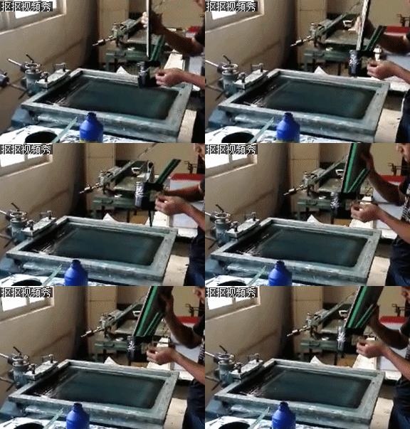
Character Screen Printing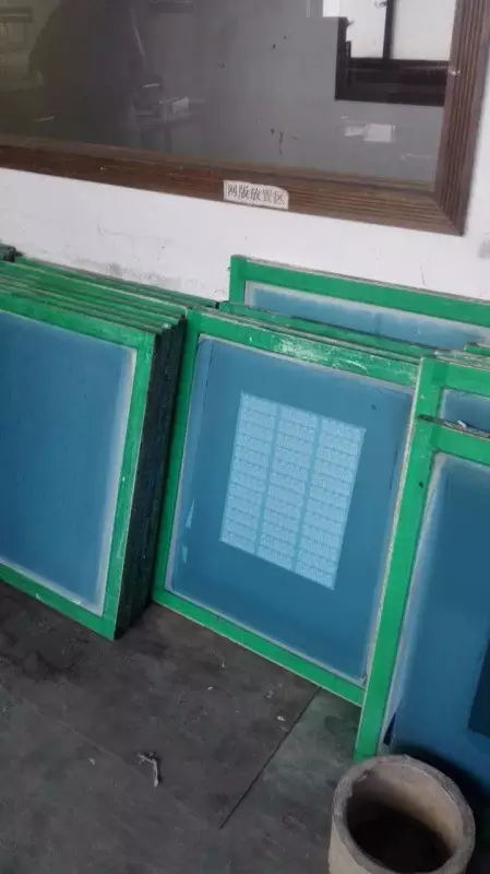
Final Step: Comprehensive Inspection
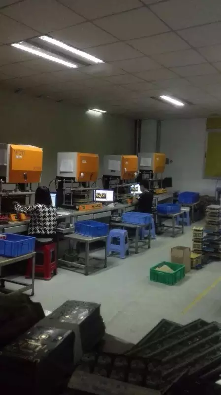
During sample processing, the factory generally does not use fixtures for testing, relying on manual testing; if in small batches, the factory needs to create testing fixtures to test the impedance and connectivity of all traces.

Some screenshots from electronic books


Some screenshots from course PPTs
【Complete Set of Hardware Learning Materials】