1. History of PCB Development
The history of PCB development is a chronicle of the continuous miniaturization, integration, and high performance of electronic technology.
1. Concept Origin (Early 20th Century): The idea of “printing” wires on a substrate was first proposed by Germans Albert Hansen and Americans Charles Ducas, laying the theoretical foundation for PCBs.
2. True Birth (1936): Austrian Paul Eisler invented the world’s first modern PCB, which was used in radio fuse devices during World War II.
3. Single-Sided Era (1950s): After the war, technology was declassified, and PCBs entered the civilian sector. Early single-sided paper substrates became mainstream, with circuits made through etching processes and components installed using through-hole technology.
4. Double-Sided and Multi-Layer (1960s): With the advent of integrated circuits, circuits became more complex, and double-sided boards and plated through-hole technology became key. Later, multi-layer boards emerged, allowing multiple circuit layers to be laminated together, achieving high-density wiring.
5. Technological Revolution (1980s to Present): Surface mount technology replaced traditional through-hole technology, resulting in smaller components and denser installations. Coupled with automated production, PCBs rapidly evolved towards high-density interconnection, flexibility, and integration, supporting the entire modern electronic information industry.
Core Evolution Path: Manual Wiring → Single-Sided Boards → Double-Sided Boards → Multi-Layer Boards → High-Density Interconnection/Flexible Boards
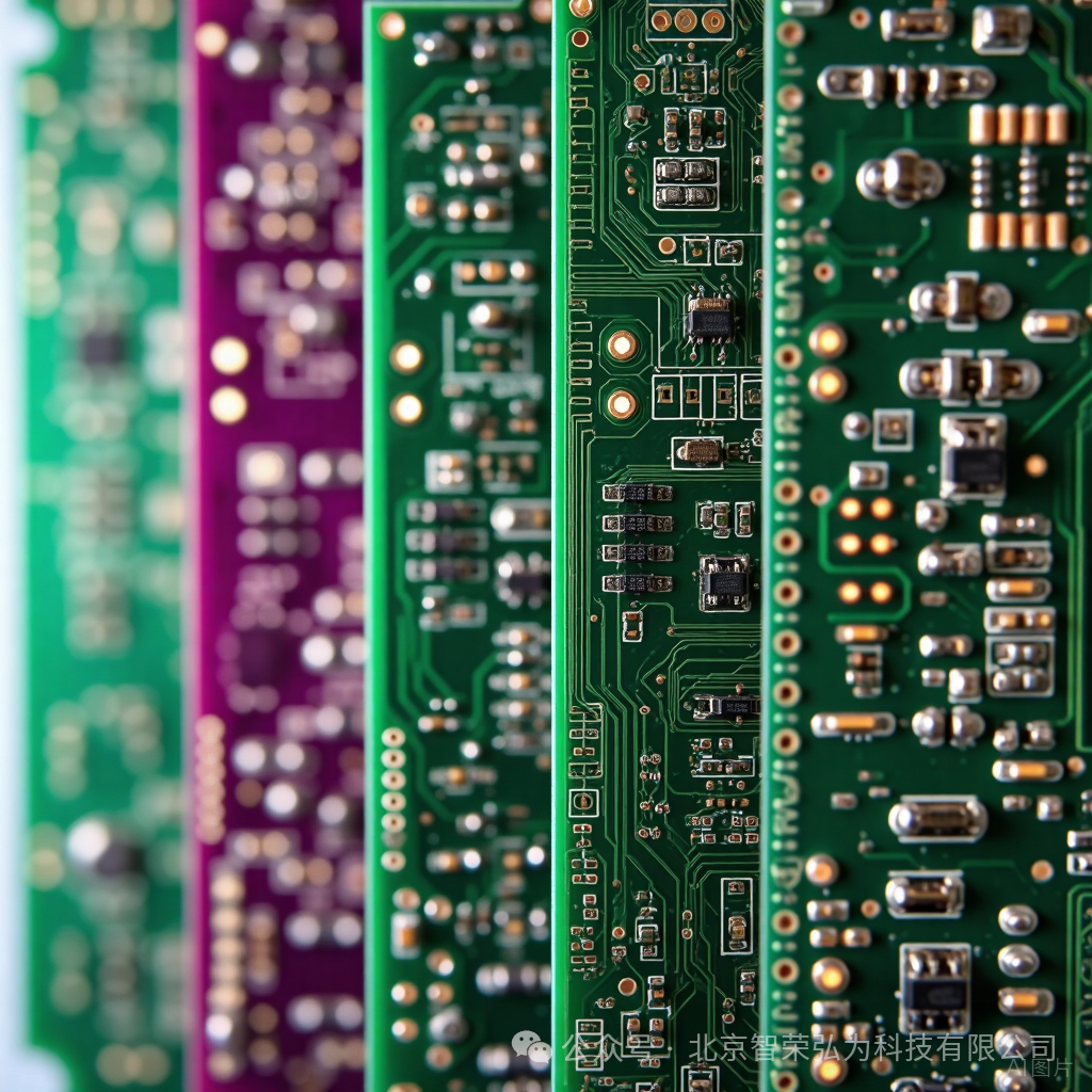 2. Types of PCBs
| Classification Method | Type | Characteristics and Applications |
| By Layer Count |
Single-Sided (Single-Sided) |
Only one side has a copper foil conductive layer, the lowest cost, used for simple circuits such as toys and remote controls. |
|
Double-Sided (Double-Sided) |
Both sides have conductive layers connected by metalized vias (VIA). This is the most common type with a wide range of applications. |
|
|
Multi-Layer (Multi-Layer) |
Composed of 3 or more conductive layers laminated together (usually an even number of layers, such as 4, 6, 8…32 layers). Used for complex circuits like motherboards, servers, and communication devices. |
|
| By Flexibility |
Rigid PCB |
Made from a rigid substrate (such as FR-4), cannot be bent. Most electronic products use rigid PCBs. |
|
Flexible PCB (FPC) |
Uses flexible substrates like polyimide, can be bent, folded, or rolled. Used in space-constrained or moving parts, such as mobile phone screens, cameras, and hard disk heads. |
|
|
Rigid-Flex PCB |
A combination of rigid and flexible boards. It combines the support of rigid areas with the flexibility of flexible areas, commonly used in high-end cameras, medical devices, and aerospace. |
|
| By Material |
FR-4 |
The most commonly used glass fiber epoxy resin copper-clad board, with good mechanical strength and insulation properties, and high cost-performance ratio. |
|
High-Frequency Board |
Uses materials with low dielectric constant and low loss factor such as PTFE and ceramic fillers, used in 5G, radar, satellite communication and other high-frequency fields. |
|
|
Metal Core PCB (MCPCB) |
The substrate is metal (usually aluminum), with excellent heat dissipation performance. Mainly used in LED lighting, power modules, and other fields requiring significant heat dissipation. |
3. Functions of PCBs
The core function of PCBs goes far beyond mere “connection”; it is a complete platform and ecosystem.
1. Provides Mechanical Support
· PCBs provide fixed mounting positions and mechanical support for various electronic components (such as chips, resistors, capacitors, connectors), making the entire circuit a solid whole rather than a tangled mess of wires.
2. Achieves Electrical Connection
· This is the most core function. The pre-designed copper foil traces (wires) on the PCB replace complex flying wires, reliably and accurately transmitting electrical signals and power between components. It determines the transmission path and integrity of the signals.
3. Achieves Specific Electrical Characteristics
· Modern high-speed PCB design is far more than just “connecting”. By precisely controlling trace width, length, spacing, stacking structure, and impedance matching, PCBs can ensure the quality of high-speed signals, reducing reflections, crosstalk, and losses, which is crucial for computers, servers, and communication devices.
4. Provides Heat Dissipation Path
· For high-power devices (such as CPUs, power amplifiers), the PCB itself can serve as a heat dissipation channel. Through **thermal vias** and large copper areas, heat can be conducted from the components to the other side of the PCB or to dedicated heat sinks. Metal core PCBs (MCPCBs) are specifically designed for heat dissipation.
5. Provides Basis for Soldering and Assembly
· The silkscreen layer on the PCB prints the outlines, labels, and polarities of components, guiding workers for quick and accurate assembly and subsequent maintenance and debugging.
In summary, PCBs have evolved from a simple connection substitute to a highly engineered, key component that determines the performance of electronic systems. They are not only the “skeleton” and “veins” of electronic components but also the “nervous system” of the entire device. Without PCBs, there would be no modern highly integrated, powerful electronic products.
Thank you for reading my article. If you found it helpful, please give me a follow! Let’s continue our discussion next time.