Senhui Introduction: Suzhou Senhui Semiconductor, supported by a strong research and technology team, focuses on providing complete process solutions and wafer processing services for global compound semiconductor customers. The company team members have been deeply involved in the semiconductor industry for many years, possessing decades of rich experience in photolithography, thin film processes, epitaxy, bonding, etching, wet processing, and polishing, with mature technology and extensive process experience.
Chiplets and Heterogeneous Packaging: SemiconductorSystem
Design’s ‘Modular Revolution’

As the R&D cost of 7nm processes exceeds $500 million and the unit price of 3nm wafers reaches $20,000, the semiconductor industry must break free from the inertia of ‘process-only’ thinking. The traditional monolithic SoC (System on Chip) ‘one-time casting’ model is being rewritten by the ‘modular puzzle’ approach of Chiplets. This revolution not only aims to solve the cost dilemma of advanced processes but also to reconstruct the underlying logic of electronic product design: from mobile phone SoCs to AI servers, from autonomous driving chips to aerospace equipment, how to achieve a balance of performance, cost, and innovation through a ‘building block’ approach has become the key to breaking the industry deadlock.
The ‘Old Path’ of System Design: The
Economic and Technical Dilemma of Traditional Monolithic Architecture
For the past half-century, the semiconductor industry has easily achieved performance leaps by ‘shrinking transistor sizes’ — this ‘process-driven’ model, however, has hit a ‘cost wall’ in the face of advanced nodes. The non-recurring engineering (NRE) cost of 5nm technology exceeds $500 million, equivalent to a small to medium-sized company ‘betting their entire fortune’ to develop a chip, while the yield issues of large silicon wafers exacerbate the situation: if there is a defect on a 12-inch wafer, the entire monolithic SoC may be scrapped, and for every 10% drop in yield, the unit cost can soar by 20%.
For low-volume fields (such as specialty chips and aerospace chips), the traditional model is an ‘unbearable burden.’ A certain aerospace chip manufacturer once calculated that to meet radiation resistance requirements, a dedicated SoC would need to be customized; if a 7nm monolithic solution were used, the R&D cost alone would be $300 million, while the annual production would only be a few thousand units, pushing the cost per unit over $100,000. In contrast, if split into ‘radiation-resistant CPU chiplet + general I/O chiplet’ architecture, the R&D cost could be reduced by 60%, and the yield could be improved to over 90%.
This economic reality forces the industry to shift towards a path of ‘beyond Moore’s Law,’ while packaging design has upgraded from ‘backend support’ to ‘frontend core,’ bringing new technical challenges:
Shift in Design Thinking: In the past, designers only needed to focus on the ‘power-performance-area (PPA)’ of a single chip; now they must consider the interconnect efficiency between multiple chiplets — for example, whether the bandwidth between CPU chiplets and GPU chiplets matches, and whether the latency of storage chiplets will slow down computation. This ‘system-level optimization’ requires a completely new design toolchain.
Skill Iteration for Packaging Engineers: Traditional packaging engineers excel in wiring design for laminated substrates, but now, facing silicon interposers, they must master chip-level physical verification processes (such as DRC/LVS rules) — the line width of silicon interposers is only 2μm, ten times finer than traditional substrates, and any design error could lead to interconnect failure.
Complexity Explosion of Thermal-Electric Coordination: In heterogeneous packaging, a 200W computing chiplet adjacent to a 10W I/O chiplet can have a local heat flux density of up to 500W/cm², equivalent to placing a soldering iron on a fingernail. Thermal analysis is no longer ‘single-chip simulation’ but requires a multi-dimensional model linking chips, packaging, PCBs, and cooling systems — tests from a certain manufacturer show that neglecting thermal coupling between chiplets can lead to actual junction temperature deviations exceeding 30°C, directly affecting chip reliability.
Part.1
The ‘Building Block Logic’ of Chiplets: Core Breakthrough from Definition to Implementation
Core Breakthrough

Chiplets are not simply ‘chip splits’ but ‘functional modules with universal interfaces’ — they decompose traditional SoCs into independent ‘compute chiplets,’ ‘storage chiplets,’ and ‘I/O chiplets,’ each chiplet is tested individually (ensuring they are ‘known good die’) and equipped with standardized communication interfaces, akin to the ‘universal snap’ of LEGO blocks, allowing flexible combinations into different systems.
The core value of this architecture lies in ‘selecting the optimal solution as needed’:
Process Mismatch: The CPU core uses a 7nm advanced process to pursue high performance, while the I/O interface uses a 28nm mature process to control costs — the AMD Ryzen 7000 series is a typical case, where the 7nm process CCD (compute chiplet) is responsible for computing power, and the 12nm process I/O Die is responsible for interfaces, reducing costs by 30% and improving yields by 40% compared to an all 7nm monolithic solution.
Technology Mixing: Chiplets made from different materials and processes can be integrated together — for example, packaging GaN (gallium nitride) RF chiplets with silicon-based compute chiplets meets the high-frequency requirements of 5G base stations without requiring the entire chip to adopt the expensive GaN process.
Rapid Iteration: Reusing mature chiplets shortens the R&D cycle — a certain AI chip manufacturer reduced the time to market for new products from 18 months to 9 months by reusing existing GPU chiplets and only developing new AI acceleration chiplets, cutting R&D investment by 50%.
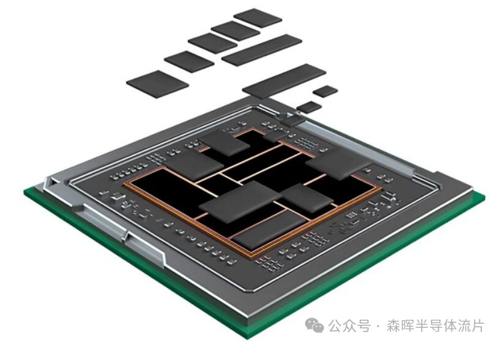
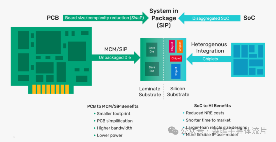
Heterogeneous integration, on the other hand, is the ‘connection technology’ that enables these ‘building blocks’ to collaborate efficiently — its essential difference from traditional SiP (System in Package) lies in ‘interconnect density’ and ‘interface standardization’:
Traditional SiP: Multiple bare chips are connected through substrate wiring, with an interconnect density of about 1000/mm² and delays exceeding 100ps, suitable for low-bandwidth scenarios (such as wearable devices).
Heterogeneous integration: Achieves high-density interconnects through silicon interposers or 3D stacking — TSMC’s CoWoS technology achieves an interconnect density of 100,000/mm², with delays reduced to under 10ps, equivalent to building a ‘nano-level highway’ between chiplets, sufficient to support the TB-level bandwidth requirements of AI chips.
Taking NVIDIA’s H100 AI chip as an example, it integrates 2 GPU chiplets and 6 HBM3 storage chiplets through CoWoS packaging, achieving an inter-chip bandwidth of 4TB/s, which is 20 times higher than traditional SiP; while Apple’s M1 Ultra directly ‘stitches’ two M1 Max chips together through a silicon interposer, achieving 2.5TB/s inter-chip interconnect, performance close to monolithic design while avoiding the yield trap of large silicon wafers.
Technological Evolution and Future Challenges: The Distance from ‘Niche Innovation’
to ‘Industry Standard’
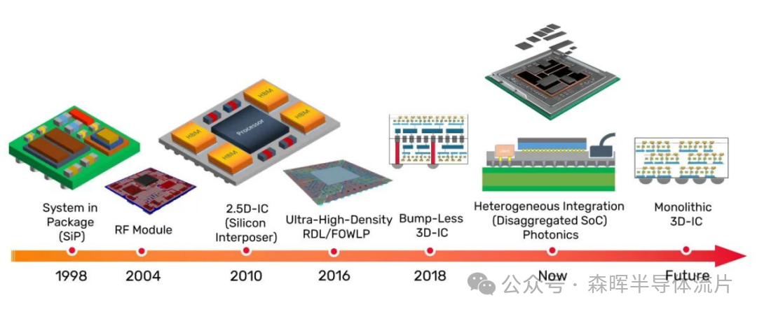
Chiplets and heterogeneous packaging are not ‘new technologies’ but the inevitable result of half a century of semiconductor packaging evolution:
1960s: Multi-Chip Modules (MCM) emerged, relying on simple stacking of bare chips to enhance integration, but limited by testing technology, resulting in very low yields;
1990s: Wafer-level testing became widespread, solving the ‘known good die’ problem, and system-in-package (SiP) began to be applied in consumer electronics;
Post-2010: Silicon interposer and TSV (Through-Silicon Via) technologies matured, leading to the emergence of 2.5D/3D packaging, achieving high-density interconnects and laying the foundation for chiplets;
Today: Standards such as UCIe (Universal Chiplet Interconnect Express) have been introduced, transitioning chiplets from ‘vendor-customized’ to ‘industry-standard,’ about to enter the stage of large-scale application.
However, to become an ‘industry standard,’ three key hurdles must be overcome:
The ‘Interface War’ of Standardization: Currently, Intel’s EMIB, TSMC’s CoWoS, and Samsung’s X-Cube interfaces are incompatible, like different brands of LEGO blocks that cannot be used interchangeably. The UCIe 3.0, set to be released in 2025, will increase the rate to 64 GT/s and support cross-vendor interconnects, but still needs to resolve details such as ‘testing standards’ and ‘thermal model formats’ — for example, how the thermal power model of chiplet A can be recognized by the system design tools of vendor B, there is currently no unified solution.
The ‘Ecological Dilemma’ of Supply Chain Maturity: Chiplets require a ‘universal chiplet library’ to support them, but currently, most chiplets are self-developed by vendors (such as NVIDIA’s GPU chiplets and AMD’s CPU chiplets), with very few third-party chiplet suppliers (such as vendors focusing on I/O and storage). Research shows that only 15% of IP vendors have commercial chiplet plans, primarily due to ‘unclear business models’ — the testing, warranty, and pricing systems for chiplets have yet to be established, and vendors are concerned about not being able to profit after investment.
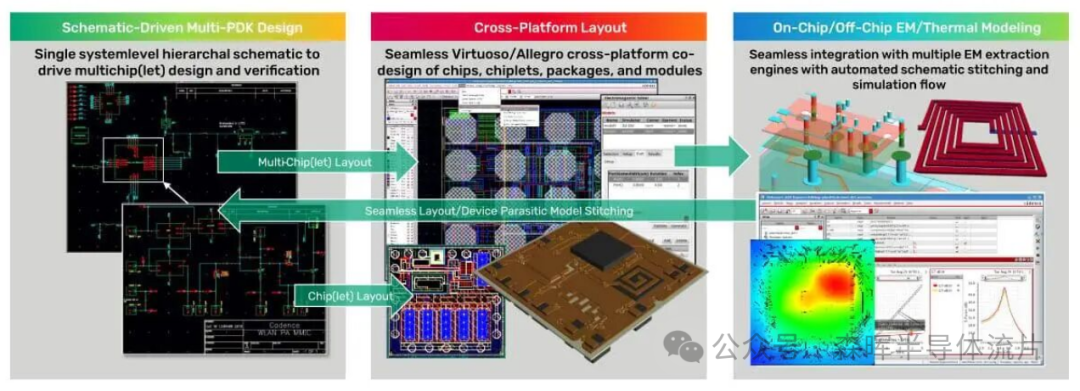
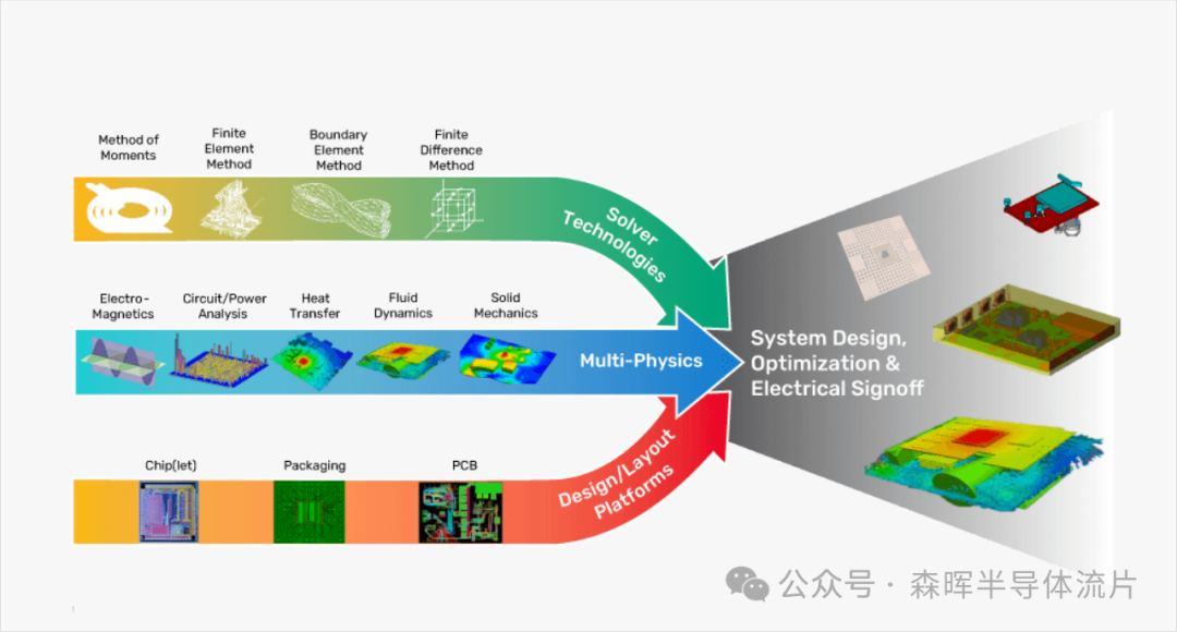
The ‘Difficulty of Collaboration’ in Design Tools: Current design tools often focus on ‘single-chip’ designs, lacking collaborative platforms across chiplets, packaging, and PCBs — for example, when laying out chiplets, it is impossible to calculate the wiring difficulty of the packaging substrate in real-time, leading to skyrocketing costs for later modifications. What the industry needs is an ‘end-to-end solution’: from chiplet selection, interconnect design, to thermal analysis and system verification, forming a unified design process, but currently, such toolchains are only being explored by a few leading vendors (such as Synopsys and Cadence).
#semiconductor#wafer#compound semiconductor#semiconductor packaging#front-end and back-end processes#semiconductor processes#etching#deposition