Wherever there is electricity, printed circuit boards (PCBs) are needed. Today, we will introduce the basic process and principles of outer layer graphic transfer. The outer layer graphic process has several names; some factories call it dry film, others call it dry film transfer, some refer to it as the outer layer, and others as outer imaging. In essence, they all mean the same thing: transferring the customer’s required outer layer circuit graphics onto the outer copper-clad board (photo copper board) using exposure and development methods.Due to the lengthy process, we will introduce it in parts, starting with this first article. Please continue reading. First, let’s outline the topics covered in this explanation, which are divided into the following six sections.
1. Introduction
2. Overview of the Process
3. Process Flow
4. Principles of the Process
5. Main Testing Items for Each Step
6. Conclusion
1. Introduction
This material covers the basic principles of the outer layer graphic transfer process, suitable for training engineers and related technical personnel responsible for the outer layer graphic transfer process, enabling them to quickly grasp the fundamental knowledge of graphic transfer and provide principled guidance for subsequent process maintenance and improvement.
2. Overview of the Process
Definition of graphic transfer:
A photosensitive film layer is applied to a treated copper surface, and under ultraviolet light, the circuit graphics from the film negative are transferred onto the copper surface, forming a mask pattern that is either etch-resistant or plating-resistant. Depending on the process, there are mainly two types of outer layer graphic transfer processes:
1) Acid etching reduction process:
The mask pattern serves as an etch-resistant layer, covering the areas where copper needs to be exposed with dry film. After development, etching, and stripping processes, the outer layer graphic is formed.
2) Graphic electroplating process:
The mask pattern serves as a plating-resistant layer, covering the bare copper areas with dry film. The substrate is etched through the stripping and etching processes.
3. Process Flow
3.1 Acid etching reduction process
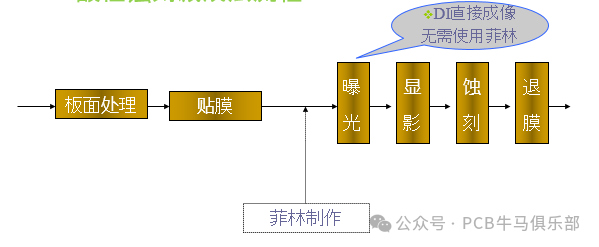
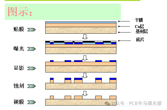
3.2 Graphic electroplating process:
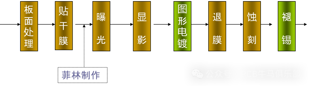
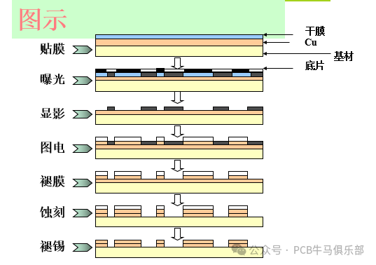
4.1: Board Surface Pre-treatment
Objective
The untreated copper surface, due to insufficient roughness and the presence of foreign substances, cannot provide adequate adhesion for the dry film. Therefore, all oxides and stains must be removed, and the surface must be microscopically roughened to increase the contact area between the dry film and the substrate surface.
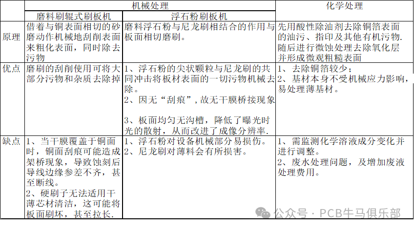
Cleaning methods
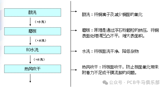
Mechanical treatment (pumice powder brushing)
Chemical treatment (degreasing + micro-etching + acid washing)
The common process for chemical treatment is as follows: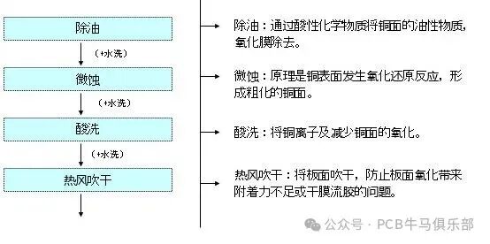
The common process for mechanical treatment is as follows:
Relationship between treated copper surface and re-oxidation
After pre-treatment, the substrate surface should be free of oxides and oil stains. However, if the retention time is too long, the surface may oxidize due to reaction with oxygen in the air. The pre-treated board should be processed within a short time.
Note: During the graphic transfer process, since the film is applied directly after pre-treatment, there is no oxidation issue on the board surface. If, for special reasons, the film cannot be applied, the production board needs to undergo pre-treatment again.
Requirements for treated copper surface
1) Chemical treatment: The roughening effect is measured by the amount of micro-etching, generally controlled between 1-2um. The surface after chemical treatment should have a uniform color, free of debris, stains, and water marks. Microscopically, the surface should be uniform and dense;
2) Mechanical treatment: The roughening effect is measured by scratches and water break points. Generally, scratches are controlled between 10-18mm, and the water break point should remain ≥30 seconds without breaking. The treated surface should have a uniform color, free of debris, stains, and water marks. Microscopically, the surface treatment may not be very uniform, but the roughening effect is deeper.
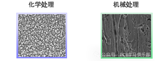
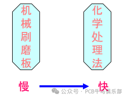
Comparison of cleaning treatment methods for board surface pre-treatment
4.2: Film Application on Board Surface
During film application, first peel off the polyethylene protective film from the dry film, and then under heated and pressurized conditions, adhere the dry film resist to the copper-clad board.
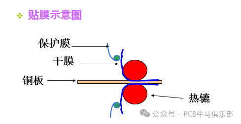
Three key factors to note during film application:Pressure, temperature, transfer speed
Requirements after film application:
The film should be smooth, without wrinkles, bubbles, or dust particles. To maintain process stability, the film should be allowed to rest for 15 minutes before exposure.
Important note:The film should be allowed to rest for 15 minutes before exposure.
Setting and impact of retention time:
The board must rest for more than 15 minutes and within 24 hours after film application. If the retention time is insufficient:
The adhesion promoter added to the dry film may not fully react with the copper, leading to poor adhesion and film loosening. If the retention time is too long, it may cause excessive reaction and strong adhesion, making development and stripping difficult.
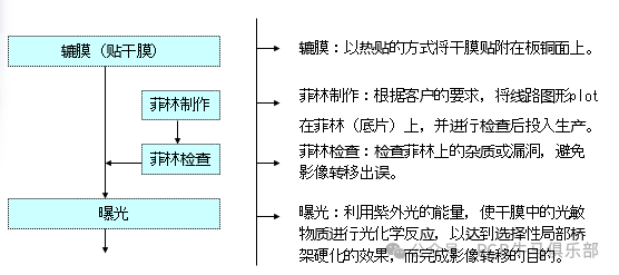
4.3 Exposure
Definition: Using photosensitive materials, the designed circuit graphics are achieved through the processes of exposure/development/etching to obtain the desired copper surface circuit graphics.
To be continued!!! Follow our public account for more exciting content!!! Click to follow so you don’t get lost!!!
Special note: The above discussion is for reference only and serves as a starting point for further exploration! Each factory’s chemicals/processes/equipment/product structures, etc., have various differences, and one must not rigidly apply these methods. All effective improvement measures come from experimental data! As a professional quality of engineering technicians, one must “speak with data.”
This public account will continue to update information related to PCB manufacturing and cutting-edge technologies.
Thank you, not only for being so good-looking and handsome but also for moving your golden fingers to get rich. Please follow, collect, like, share, and leave comments!!!
Original content is not easy; if you want to reprint, please message the author for permission and indicate the source before reprinting. Thank you for your cooperation!